- 您現在的位置:買賣IC網 > PDF目錄373961 > AD9226 (Analog Devices, Inc.) Complete 12-Bit, 65 MSPS ADC Converter PDF資料下載
參數資料
| 型號: | AD9226 |
| 廠商: | Analog Devices, Inc. |
| 英文描述: | Complete 12-Bit, 65 MSPS ADC Converter |
| 中文描述: | 完整的12位,65 MSPS的ADC轉換 |
| 文件頁數: | 19/28頁 |
| 文件大小: | 1480K |
| 代理商: | AD9226 |
第1頁第2頁第3頁第4頁第5頁第6頁第7頁第8頁第9頁第10頁第11頁第12頁第13頁第14頁第15頁第16頁第17頁第18頁當前第19頁第20頁第21頁第22頁第23頁第24頁第25頁第26頁第27頁第28頁
REV. 0
AD9226
–19–
stopped. Once the clock frequency is changed, over 100 clock
cycles may be required for the clock stabilizer to settle to a dif-
ferent speed. When the stabilizer is disabled, the internal switching
will be directly affected by the clock state. If the external clock is
high, the SHA will be in hold. If the clock pulse is low, the SHA
will be in track. TPC 16 shows the benefits of using the clock
stabilizer. See Tables I and III.
Data Format Select (DFS)
The AD9226 may be set for binary or two
’
s complement data
output formats. See Tables I and II.
SSOP Package
The SSOP mode control (Pin 22) has two functions. It enables/
disables the clock stabilizer and determines the output data format.
The exact functions of the mode pin are outlined in Table I.
Table I. Mode Select (SSOP)
Mode
DFS
Clock Duty Cycle Shaping
DNC
AVDD
GND
10 k
Resistor
Binary
Binary
Two
’
s Complement
Two
’
s Complement
To GND
Clock Stabilizer Disabled
Clock Stabilizer Enabled
Clock Stabilizer Enabled
Clock Stabilizer Disabled
LQFP Package
Pin 35 of the LQFP package determines the output data format
(DFS). If it is connected to AVSS, the output word will be straight
binary. If it is connected to AVDD, the output data format will
be two
’
s complement. See Table II.
Pin 43 of the LQFP package controls the clock stabilizer function
of the AD9226. If the pin is connected to AVDD, both clock
edges will be used in the conversion architecture. When Pin 43
is connected to AVSS, the internal duty cycle will be determined
by the clock stabilizer function within the ADC. See Table III.
Table II. DFS Pin Controls
DFS Function
Pin 35 Connection
Straight Binary
Two
’
s Complement
AVDD
AVSS
Table III. Clock Stabilizer Pin
Clock Restore Function
Pin 43 Connection
Clock Stabilizer Enabled
Clock Stabilizer Disabled
AVDD
AVSS
DIGITAL INPUTS AND OUTPUTS
Digital Outputs
Table IV details the relationship among the ADC input, OTR, and
straight binary output.
Table IV. Output Data Format
Two’s
Complement
Mode
Binary
Output Mode
Input (V)
Condition (V)
OTR
VINA
–
VINB <
–
VREF
VINA
–
VINB =
–
VREF
VINA
–
VINB = 0
VINA
–
VINB = + VREF
–
1 LSB 1111 1111 1111
VINA
–
VINB
≥
+ VREF
0000 0000 0000
0000 0000 0000
1000 0000 0000
1000 0000 0000
1000 0000 0000
0000 0000 0000
0111 1111 1111
0111 1111 1111
1
0
0
0
1
1111 1111 1111
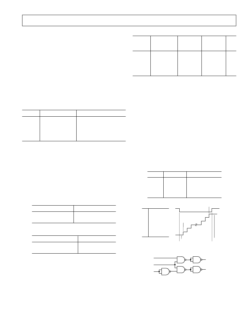
Out of Range (OTR)
An out-of-range condition exists when the analog input voltage
is beyond the input range of the converter. OTR is a digital
output that is updated along with the data output corresponding
to the particular sampled analog input voltage. Hence, OTR has
the same pipeline delay (latency) as the digital data. It is LOW
when the analog input voltage is within the analog input range.
It is HIGH when the analog input voltage exceeds the input
range as shown in Figure 14. OTR will remain HIGH until the
analog input returns within the input range and another conversion
is completed. By logical ANDing OTR with the MSB and its
complement, overrange high or underrange low conditions can be
detected. Table V is a truth table for the over/underrange
circuit in Figure 15, which uses NAND gates. Systems requiring
programmable gain conditioning of the AD9226 input signal
can immediately detect an out-of-range condition, thus elimi-
nating gain selection iterations. Also, OTR can be used for
digital offset and gain calibration.
Table V. Out-of-Range Truth Table
OTR
0
0
1
1
MSB
0
1
0
1
Analog Input Is
In Range
In Range
Underrange
Overrange
1111 1111 1111
1111 1111 1111
1111 1111 1110
OTR
–
FS
+FS
–
FS +1/2 LSB
+FS
–
1/2 LSB
–
FS
–
1/2 LSB
+FS
–
1 1/2 LSB
0000 0000 0001
0000 0000 0000
0000 0000 0000
1
0
0
0
0
1
OTR DATA OUTPUTS
Figure 14. OTR Relation to Input Voltage and Output Data
OVER = 1
UNDER = 1
MSB
OTR
MSB
Figure 15. Overrange or Underrange Logic
相關PDF資料 |
PDF描述 |
|---|---|
| AD9226-EB | Complete 12-Bit, 65 MSPS ADC Converter |
| AD9226AST | Complete 12-Bit, 65 MSPS ADC Converter |
| AD9226ARS | Complete 12-Bit, 65 MSPS ADC Converter |
| AD9228 | Quad, 12-bit, 40/65 MSPS Serial LVDS 1.8 V A/D Converter |
| AD9228-65EB | Quad, 12-bit, 40/65 MSPS Serial LVDS 1.8 V A/D Converter |
相關代理商/技術參數 |
參數描述 |
|---|---|
| AD9226_01 | 制造商:AD 制造商全稱:Analog Devices 功能描述:Complete 12-Bit, 65 MSPS ADC Converter |
| AD9226ARS | 功能描述:IC ADC 12BIT 65MSPS 28-SSOP RoHS:否 類別:集成電路 (IC) >> 數據采集 - 模數轉換器 系列:- 產品培訓模塊:Lead (SnPb) Finish for COTS Obsolescence Mitigation Program 標準包裝:2,500 系列:- 位數:12 采樣率(每秒):3M 數據接口:- 轉換器數目:- 功率耗散(最大):- 電壓電源:- 工作溫度:- 安裝類型:表面貼裝 封裝/外殼:SOT-23-6 供應商設備封裝:SOT-23-6 包裝:帶卷 (TR) 輸入數目和類型:- |
| AD9226ARSRL | 功能描述:IC ADC 12BIT 65MSPS 28-SSOP RoHS:否 類別:集成電路 (IC) >> 數據采集 - 模數轉換器 系列:- 產品培訓模塊:Lead (SnPb) Finish for COTS Obsolescence Mitigation Program 標準包裝:2,500 系列:- 位數:12 采樣率(每秒):3M 數據接口:- 轉換器數目:- 功率耗散(最大):- 電壓電源:- 工作溫度:- 安裝類型:表面貼裝 封裝/外殼:SOT-23-6 供應商設備封裝:SOT-23-6 包裝:帶卷 (TR) 輸入數目和類型:- |
| AD9226ARSZ | 功能描述:IC ADC 12BIT 65MSPS 28-SSOP RoHS:是 類別:集成電路 (IC) >> 數據采集 - 模數轉換器 系列:- 標準包裝:1 系列:- 位數:14 采樣率(每秒):83k 數據接口:串行,并聯 轉換器數目:1 功率耗散(最大):95mW 電壓電源:雙 ± 工作溫度:0°C ~ 70°C 安裝類型:通孔 封裝/外殼:28-DIP(0.600",15.24mm) 供應商設備封裝:28-PDIP 包裝:管件 輸入數目和類型:1 個單端,雙極 |
| AD9226ARSZRL | 功能描述:IC ADC 12BIT 65MSPS 28SSOP RoHS:是 類別:集成電路 (IC) >> 數據采集 - 模數轉換器 系列:- 標準包裝:1 系列:- 位數:14 采樣率(每秒):83k 數據接口:串行,并聯 轉換器數目:1 功率耗散(最大):95mW 電壓電源:雙 ± 工作溫度:0°C ~ 70°C 安裝類型:通孔 封裝/外殼:28-DIP(0.600",15.24mm) 供應商設備封裝:28-PDIP 包裝:管件 輸入數目和類型:1 個單端,雙極 |
發布緊急采購,3分鐘左右您將得到回復。