- 您現在的位置:買賣IC網 > PDF目錄373961 > AD9226AST (ANALOG DEVICES INC) Complete 12-Bit, 65 MSPS ADC Converter PDF資料下載
參數資料
| 型號: | AD9226AST |
| 廠商: | ANALOG DEVICES INC |
| 元件分類: | ADC |
| 英文描述: | Complete 12-Bit, 65 MSPS ADC Converter |
| 中文描述: | 1-CH 12-BIT FLASH METHOD ADC, PARALLEL ACCESS, PQFP48 |
| 封裝: | PLASTIC, LQFP-48 |
| 文件頁數: | 18/28頁 |
| 文件大小: | 1480K |
| 代理商: | AD9226AST |
第1頁第2頁第3頁第4頁第5頁第6頁第7頁第8頁第9頁第10頁第11頁第12頁第13頁第14頁第15頁第16頁第17頁當前第18頁第19頁第20頁第21頁第22頁第23頁第24頁第25頁第26頁第27頁第28頁
REV. 0
AD9226
–18–
A2
LOGIC
A1
DISABLE
A1
1V
TO
A/D
AD9226
CAPT
CAPB
VREF
SENSE
REFCOM
2.5V
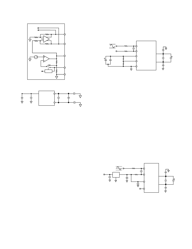
Figure 11a. Equivalent Reference Circuit
0.1 F
10 F
0.1 F
0.1 F
CAPT
CAPB
AD9226
VREF
0.1 F
10 F
Figure 11b. CAPT and CAPB DC-Coupling
The actual reference voltages used by the internal circuitry of the
AD9226 appear on the CAPT and CAPB pins. The voltages
on these pins are symmetrical about the analog supply. For
proper operation when using an internal or external reference, it
is necessary to add a capacitor network to decouple these pins.
Figure 11b shows the recommended decoupling network. The
turn-on time of the reference voltage appearing between CAPT
and CAPB is approximately 10 ms and should be evaluated in
any power-down mode of operation.
USING THE INTERNAL REFERENCE
The AD9226 can be easily configured for either a 1 V p-p input
span or 2 V p-p input span by setting the internal reference.
Other input spans can be realized with two external gain-
setting resistors as shown in Figure 12 of this data sheet, or
using an external reference.
Pin Programmable Reference
By shorting the VREF pin directly to the SENSE pin, the inter-
nal reference amplifier is placed in a unity-gain mode and the
resultant VREF output is 1 V. By shorting the SENSE pin
directly to the REFCOM pin, the internal reference amplifier is
configured for a gain of 2.0 and the resultant VREF output is
2.0 V. The VREF pin should be bypassed to the REFCOM pin
with a 10
μ
F tantalum capacitor in parallel with a low-inductance
0.1
μ
F ceramic capacitor as shown in Figure 11b.
Resistor Programmable Reference
Figure 12 shows an example of how to generate a reference
voltage other than 1.0 V or 2.0 V with the addition of two exter-
nal resistors. Use the equation,
VREF
= 1
V
×
(1 +
R
1/
R
2)
to determine appropriate values for
R
1 and
R
2. These resistors
should be in the 2 k
to 10 k
range. For the example shown,
R1 equals 2.5 k
and R2 equals 5 k
. From the equation above,
the resultant reference voltage on the VREF pin is 1.5 V. This
sets the input span to be 1.5 V p-p. The midscale voltage can
also be set to VREF by connecting VINB to VREF. Alterna-
tively, the midscale voltage can be set to 2.5 V by connecting
VINB to a low-impedance 2.5 V source as shown in Figure 12.
VINA
VREF
AD9226
VINB
1.75V
SENSE
REFCOM
0.1 F
10 F
0.1 F
0.1 F
15pF
3.25V
33
33
1.5V
0.1 F
CAPT
2.5V
10 F
R1
2.5k
R2
5k
CAPB
0.1C1
Figure 12. Resistor Programmable Reference (1.5 V p-p
Input Span, Differential Input V
CM
= 2.5 V)
USING AN EXTERNAL REFERENCE
The AD9226 contains an internal reference buffer, A2 (see
Figure 11b), that simplifies the drive requirements of an external
reference. The external reference must be able to drive about
5 k
(
±
20%) load. Note that the bandwidth of the reference
buffer is deliberately left small to minimize the reference noise
contribution. As a result, it is not possible to rapidly change the
reference voltage in this mode.
Figure 13 shows an example of an external reference driving
both VINB and VREF. In this case, both the common-mode
voltage and input span are directly dependent on the value of
VREF. Both the input span and the center of the input span are
equal to the external VREF. Thus the valid input range extends
from (VREF + VREF/2) to (VREF
–
VREF/2). For example,
if the REF191, a 2.048 V external reference, is selected, the
input span extends to 2.048 V. In this case, 1 LSB of the AD9226
corresponds to 0.5 mV. It is essential that a minimum of a 10
μ
F
capacitor, in parallel with a 0.1
μ
F low-inductance ceramic
capacitor, decouple the reference output to ground.
To use an external reference, the SENSE pin must be connected
to AVDD. This connection will disable the internal reference.
VINA
VREF
AD9226
VINB
SENSE
0.1 F
10 F
0.1 F
0.1 F
15pF
VINA+VREF/2
33
33
0.1 F
CAPT
CAPB
VINB
–
VREF/2
10 F
VREF
0.1 F
5V
5V
Figure 13. Using an External Reference
MODE CONTROLS
Clock Stabilizer
The clock stabilizer is a circuit that desensitizes the ADC from
clock duty cycle variations. The AD9226 eases system clock
constraints by incorporating a circuit that restores the internal duty
cycle to 50%, independent of the input duty cycle. Low jitter on
the rising edge (sampling edge) of the clock is preserved while
the noncritical falling edge is generated on-chip.
It may be desirable to disable the clock stabilizer, and may be
necessary when the clock frequency speed is varied or completely
相關PDF資料 |
PDF描述 |
|---|---|
| AD9226ARS | Complete 12-Bit, 65 MSPS ADC Converter |
| AD9228 | Quad, 12-bit, 40/65 MSPS Serial LVDS 1.8 V A/D Converter |
| AD9228-65EB | Quad, 12-bit, 40/65 MSPS Serial LVDS 1.8 V A/D Converter |
| AD9229BCP-50 | Quad 12-Bit, 50/65 MSPS Serial LVDS 3V A/D Converter |
| AD9229BCP-65 | Quad 12-Bit, 50/65 MSPS Serial LVDS 3V A/D Converter |
相關代理商/技術參數 |
參數描述 |
|---|---|
| AD9226ASTRL | 功能描述:IC ADC 12BIT 65MSPS 48-LQFP RoHS:否 類別:集成電路 (IC) >> 數據采集 - 模數轉換器 系列:- 產品培訓模塊:Lead (SnPb) Finish for COTS Obsolescence Mitigation Program 標準包裝:2,500 系列:- 位數:12 采樣率(每秒):3M 數據接口:- 轉換器數目:- 功率耗散(最大):- 電壓電源:- 工作溫度:- 安裝類型:表面貼裝 封裝/外殼:SOT-23-6 供應商設備封裝:SOT-23-6 包裝:帶卷 (TR) 輸入數目和類型:- |
| AD9226ASTZ | 功能描述:IC ADC 12BIT 65MSPS 48-LQFP RoHS:是 類別:集成電路 (IC) >> 數據采集 - 模數轉換器 系列:- 標準包裝:1 系列:microPOWER™ 位數:8 采樣率(每秒):1M 數據接口:串行,SPI? 轉換器數目:1 功率耗散(最大):- 電壓電源:模擬和數字 工作溫度:-40°C ~ 125°C 安裝類型:表面貼裝 封裝/外殼:24-VFQFN 裸露焊盤 供應商設備封裝:24-VQFN 裸露焊盤(4x4) 包裝:Digi-Reel® 輸入數目和類型:8 個單端,單極 產品目錄頁面:892 (CN2011-ZH PDF) 其它名稱:296-25851-6 |
| AD9226ASTZRL | 功能描述:IC ADC 12BIT 65MSPS 48LQFP RoHS:是 類別:集成電路 (IC) >> 數據采集 - 模數轉換器 系列:- 標準包裝:1 系列:- 位數:14 采樣率(每秒):83k 數據接口:串行,并聯 轉換器數目:1 功率耗散(最大):95mW 電壓電源:雙 ± 工作溫度:0°C ~ 70°C 安裝類型:通孔 封裝/外殼:28-DIP(0.600",15.24mm) 供應商設備封裝:28-PDIP 包裝:管件 輸入數目和類型:1 個單端,雙極 |
| AD9226-EB | 制造商:Analog Devices 功能描述:EVAL BD FOR AD9226 ADC CNVRTR - Bulk |
| AD9226-LQFP-EB | 制造商:AD 制造商全稱:Analog Devices 功能描述:Complete 12-Bit, 65 MSPS ADC Converter |
發布緊急采購,3分鐘左右您將得到回復。