- 您現在的位置:買賣IC網 > PDF目錄373961 > AD9236BRUZRL7-80 (ANALOG DEVICES INC) 12-Bit, 80 MSPS, 3V A/D Converter PDF資料下載
參數資料
| 型號: | AD9236BRUZRL7-80 |
| 廠商: | ANALOG DEVICES INC |
| 元件分類: | ADC |
| 英文描述: | 12-Bit, 80 MSPS, 3V A/D Converter |
| 中文描述: | 1-CH 12-BIT FLASH METHOD ADC, PARALLEL ACCESS, PDSO28 |
| 封裝: | LEAD FREE, MO-153AE, TSSOP-28 |
| 文件頁數: | 15/36頁 |
| 文件大小: | 2056K |
| 代理商: | AD9236BRUZRL7-80 |
第1頁第2頁第3頁第4頁第5頁第6頁第7頁第8頁第9頁第10頁第11頁第12頁第13頁第14頁當前第15頁第16頁第17頁第18頁第19頁第20頁第21頁第22頁第23頁第24頁第25頁第26頁第27頁第28頁第29頁第30頁第31頁第32頁第33頁第34頁第35頁第36頁
AD9236
input span of 2 V p-p. The relative SNR degradation is 3 dB
when changing from 2 V p-p mode to 1 V p-p mode.
03600-0-014
AD9236
VIN+
VIN–
AVDD
AGND
33
33
10pF
49.9
1k
1k
0.1
μ
F
2V p-p
The SHA may be driven from a source that keeps the signal
peaks within the allowable range for the selected reference volt-
age. The minimum and maximum common-mode input levels
are defined as
2
VREF
VCM
MIN
=
(
)
2
VREF
AVDD
VCM
MAX
+
=
The minimum common-mode input level allows the AD9236 to
accommodate ground referenced inputs.
Although optimum performance is achieved with a differential
input, a single-ended source may be applied to VIN+ or VIN–.
In this configuration, one input accepts the signal, while the
opposite input should be set to midscale by connecting it to an
appropriate reference. For example, a 2 V p-p signal may be
applied to VIN+ while a 1 V reference is applied to VIN–. The
AD9236 then accepts an input signal varying between 2 V and
0 V. In the single-ended configuration, distortion performance
may degrade significantly as compared to the differential case.
However, the effect is less noticeable at lower input frequencies.
Differential Input Configurations
As previously detailed, optimum performance is achieved while
driving the AD9236 in a differential input configuration. For
baseband applications, the AD8138 differential driver provides
excellent performance and a flexible interface to the ADC. The
output common-mode voltage of the AD8138 is easily set to
AVDD/2, and the driver can be configured in a Sallen Key filter
topology to provide band limiting of the input signal.
AD9236
VIN+
VIN–
AGND
AVDD
1V p-p
49.9
523
1k
1k
0.1
μ
F
33
33
20pF
499
499
499
AD8138
03066-0-013
Figure 28. Differential Input Configuration Using the AD8138
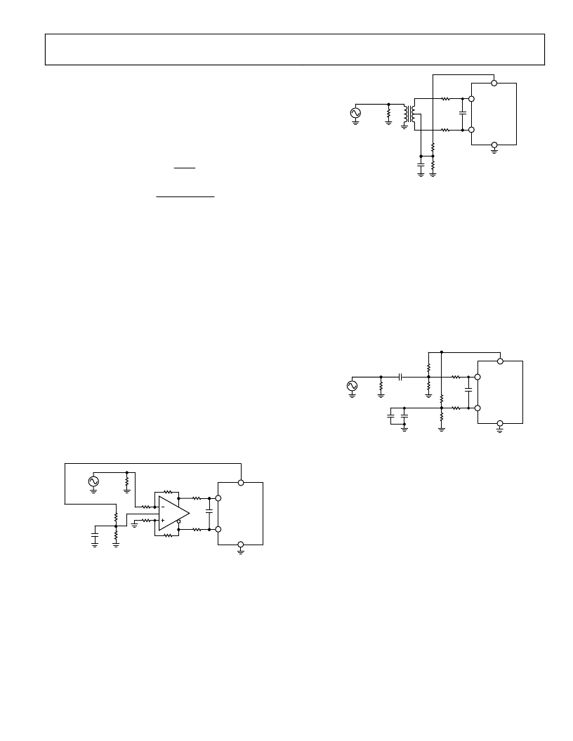
At input frequencies in the second Nyquist zone and above, the
performance of most amplifiers is not adequate to achieve the
true performance of the AD9236. This is especially true in IF
undersampling applications where frequencies in the 70 MHz
to 100 MHz range are being sampled. For these applications,
differential transformer coupling is the recommended input
configuration. The value of the shunt capacitor is dependent
on the input frequency and source impedance and should be
reduced or removed. An example is shown in F
.
igure 29
Figure 29. Differential Transformer-Coupled Configuration
The signal characteristics must be considered when selecting
a transformer. Most RF transformers saturate at frequencies
below a few MHz, and excessive signal power can also cause
core saturation, which leads to distortion.
Single-Ended Input Configuration
A single-ended input may provide adequate performance in
cost-sensitive applications. In this configuration, there is a deg-
radation in SFDR and distortion performance due to the large
input common-mode swing (see F
source impedances on each input are matched, there should be
little effect on SNR performance. F
gle-ended input configuration.
). However, if the
details a typical sin-
igure 30
igure 14
Figure 22
Figure 30. Single-Ended Input Configuration
03600-A-015
AD9236
VIN+
VIN–
AVDD
AGND
2V p-p
33
33
20pF
49.9
1k
1k
0.33
μ
F
10
μ
F
0.1
μ
F
1k
1k
+
CLOCK INPUT CONSIDERATIONS
Typical high speed ADCs use both clock edges to generate a
variety of internal timing signals, and as a result may be sensi-
tive to clock duty cycle. Commonly a 5% tolerance is required
on the clock duty cycle to maintain dynamic performance char-
acteristics. The AD9236 contains a clock duty cycle stabilizer
(DCS) that retimes the nonsampling edge, providing an internal
clock signal with a nominal 50% duty cycle. This allows a wide
range of clock input duty cycles without affecting the perform-
ance of the AD9236. As shown in
tion performance is nearly flat for a 30% to 70% duty cycle with
the DCS on.
, noise and distor-
The duty cycle stabilizer uses a delay-locked loop (DLL) to cre-
ate the nonsampling edge. As a result, any changes to the sam-
pling frequency require approximately 100 clock cycles to allow
the DLL to acquire and lock to the new rate.
Rev. A | Page 15 of 36
相關PDF資料 |
PDF描述 |
|---|---|
| AD9236BRU-80 | 12-Bit, 80 MSPS, 3V A/D Converter |
| AD9236BRU-80EB | 12-Bit, 80 MSPS, 3V A/D Converter |
| AD9238 | 12-Bit, 20/40/65 MSPS Dual A/D Converter |
| AD9238BST-20 | TV07RW21-35SD W/ PC CONT |
| AD9238BST-40 | 12-Bit, 20/40/65 MSPS Dual A/D Converter |
相關代理商/技術參數 |
參數描述 |
|---|---|
| AD9237 | 制造商:AD 制造商全稱:Analog Devices 功能描述:12-Bit, 20 MSPS/40 MSPS/65 MSPS 3 V Low Power A/D Converter |
| AD9237BCP-20EB | 制造商:Analog Devices 功能描述:12 BIT 3V 20 MSPS LOW POWER ADC - Trays |
| AD9237BCP-40EB | 制造商:Analog Devices 功能描述:12-BIT 3V 40 MSPS LOW POWER ADC - Trays |
| AD9237BCP-65EB | 制造商:Analog Devices 功能描述:12-BIT 3V 65 MSPS LOW POWER ADC - Boxed Product (Development Kits) |
| AD9237BCPZ-20 | 功能描述:IC ADC 12BIT SGL 20MSPS 32LFCSP RoHS:是 類別:集成電路 (IC) >> 數據采集 - 模數轉換器 系列:- 產品培訓模塊:Lead (SnPb) Finish for COTS Obsolescence Mitigation Program 標準包裝:2,500 系列:- 位數:12 采樣率(每秒):3M 數據接口:- 轉換器數目:- 功率耗散(最大):- 電壓電源:- 工作溫度:- 安裝類型:表面貼裝 封裝/外殼:SOT-23-6 供應商設備封裝:SOT-23-6 包裝:帶卷 (TR) 輸入數目和類型:- |
發布緊急采購,3分鐘左右您將得到回復。