- 您現在的位置:買賣IC網 > PDF目錄373961 > AD9240 (Analog Devices, Inc.) Complete 14-Bit, 10 MSPS Monolithic A/D Converter PDF資料下載
參數資料
| 型號: | AD9240 |
| 廠商: | Analog Devices, Inc. |
| 英文描述: | Complete 14-Bit, 10 MSPS Monolithic A/D Converter |
| 中文描述: | 完整的14位,10 MSPS的單片機的A / D轉換器 |
| 文件頁數: | 18/24頁 |
| 文件大小: | 328K |
| 代理商: | AD9240 |
AD9240
REV. A
–18–
Variable Input Span with V
CM
= 2.5 V
Figure 42 shows an example of the AD9240 configured for an
input span of 2
×
VREF centered at 2.5 V. An external 2.5 V
reference drives the VINB pin thus setting the common-mode
voltage at 2.5 V. The input span can be independently set by a
voltage divider consisting of R1 and R2, which generates the
VREF signal. A1 buffers this resistor network and drives VREF.
Choose this op amp based on accuracy requirements. It is
essential that a minimum of a 10
μ
F capacitor in parallel with a
0.1
μ
F low inductance ceramic capacitor decouple the reference
output to ground.
2.5V+VREF
2.5V–VREF
2.5V
+5V
0.1
m
F
22
m
F
VINA
VINB
VREF
SENSE
AD9240
+5V
R2
0.1
m
F
A1
R1
0.1
m
F
2.5V
REF
Figure 42. External Reference, V
CM
= 2.5 V (2.5 V on VINB,
Resistor Divider to Make VREF)
Single-Ended Input with 0 to 2
3
VREF Range
Figure 43 shows an example of an external reference driving
both VINB and VREF. In this case, both the common mode
voltage and input span are directly dependent on the value of
VREF. More specifically, the common-mode voltage is equal to
VREF while the input span is equal to 2
×
VREF. Thus, the
valid input range extends from 0 to 2
×
VREF. If, for example,
the REF191, a 2.048 external reference, were selected, the valid
input range extends from 0 V to 4.096 V. In this case, 1 LSB of
the AD9240 corresponds to 0.250 mV. It is essential that a
minimum of a 10
μ
F capacitor in parallel with a 0.1
μ
F low induc-
tance ceramic capacitor decouple the reference output to ground.
2xREF
0V
+5V
10
m
F
VINA
VINB
VREF
SENSE
AD9240
+5V
0.1
m
F
VREF
0.1
m
F
0.1
m
F
Figure 43. Input Range = 0 V to 2
×
VREF
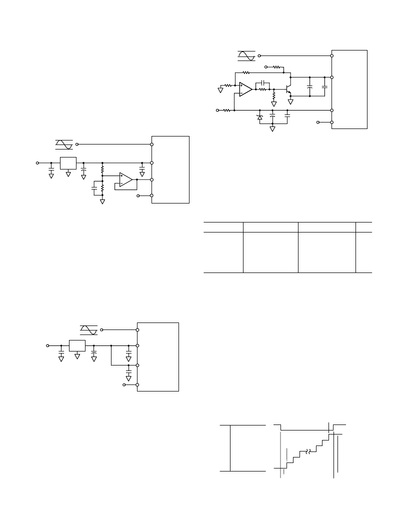
Low Cost/Power Reference
The external reference circuit shown in Figure 44 uses a low cost
1.225 V external reference (e.g., AD580 or AD1580) along with an
op amp and transistor. The 2N2222 transistor acts in conjunction
with 1/2 of an OP282 to provide a very low impedance drive for
VINB. The selected op amp need not be a high speed op amp and
may be selected based on cost, power and accuracy.
3.75V
1.25V
+5V
10
m
F
VINA
VINB
VREF
SENSE
AD9240
+5V
0.1
m
F
316
V
1k
V
0.1
m
F
1/2
OP282
10
m
F
0.1
m
F
7.5k
V
AD1580
1k
V
1k
V
820
V
+5V
2N2222
1.225V
Figure 44. External Reference Using the AD1580 and Low
Impedance Buffer
DIGITAL INPUTS AND OUTPUTS
Digital Outputs
The AD9240 output data is presented in positive true straight
binary for all input ranges. Table IV indicates the output data
formats for various input ranges regardless of the selected input
range. A twos complement output data format can be created by
inverting the MSB.
Table IV. Output Data Format
Input (V)
Condition (V)
Digital Output
OTR
VINA – VINB < –VREF
VINA – VINB = –VREF
VINA – VINB = 0
VINA – VINB = +VREF – 1 LSB
VINA – VINB
≥
+VREF
00 0000 0000 0000 1
00 0000 0000 0000 0
10 0000 0000 0000 0
11 1111 1111 1111 0
11 1111 1111 1111 1
Out Of Range (OTR)
An out-of-range condition exists when the analog input voltage
is beyond the input range of the converter. OTR is a digital
output that is updated along with the data output corresponding
to the particular sampled analog input voltage. Hence, OTR
has the same pipeline delay (latency) as the digital data. It is
LOW when the analog input voltage is within the analog input
range. It is HIGH when the analog input voltage exceeds the
input range as shown in Figure 45. OTR will remain HIGH
until the analog input returns within the input range and an-
other conversion is completed. By logical ANDing OTR with
the MSB and its complement, overrange high or underrange low
conditions can be detected. Table V is a truth table for the over/
underrange circuit in Figure 46 which uses NAND gates. Sys-
tems requiring programmable gain conditioning of the AD9240
input signal can immediately detect an out-of-range condition,
thus eliminating gain selection iterations. Also, OTR can be
used for digital offset and gain calibration.
111111 1111 1111
111111 1111 1111
111111 1111 1110
OTR
–FS
+FS
–FS+1/2 LSB
+FS –1/2 LSB
–FS –1/2 LSB
+FS –1 1/2 LSB
000000 0000 0001
000000 0000 0000
000000 0000 0000
1
0
0
0
0
1
OTR
DATA OUTPUTS
Figure 45. Output Data Format
相關PDF資料 |
PDF描述 |
|---|---|
| AD9240AS | Complete 14-Bit, 10 MSPS Monolithic A/D Converter |
| AD9240EB | Complete 14-Bit, 10 MSPS Monolithic A/D Converter |
| AD9241 | Complete 14-Bit, 1.25 MSPS Monolithic A/D Converter |
| AD9241AS | RES., MF, 2K, 1%, 1/4W |
| AD9241EB | Complete 14-Bit, 1.25 MSPS Monolithic A/D Converter |
相關代理商/技術參數 |
參數描述 |
|---|---|
| AD9240AS | 功能描述:IC ADC 14BIT 10MSPS 44-MQFP RoHS:否 類別:集成電路 (IC) >> 數據采集 - 模數轉換器 系列:- 標準包裝:1 系列:- 位數:14 采樣率(每秒):83k 數據接口:串行,并聯 轉換器數目:1 功率耗散(最大):95mW 電壓電源:雙 ± 工作溫度:0°C ~ 70°C 安裝類型:通孔 封裝/外殼:28-DIP(0.600",15.24mm) 供應商設備封裝:28-PDIP 包裝:管件 輸入數目和類型:1 個單端,雙極 |
| AD9240ASRL | 功能描述:IC ADC 14BIT 10MSPS 44-MQFP RoHS:否 類別:集成電路 (IC) >> 數據采集 - 模數轉換器 系列:- 標準包裝:1 系列:- 位數:14 采樣率(每秒):83k 數據接口:串行,并聯 轉換器數目:1 功率耗散(最大):95mW 電壓電源:雙 ± 工作溫度:0°C ~ 70°C 安裝類型:通孔 封裝/外殼:28-DIP(0.600",15.24mm) 供應商設備封裝:28-PDIP 包裝:管件 輸入數目和類型:1 個單端,雙極 |
| AD9240ASZ | 功能描述:IC ADC 14BIT 10MSPS 44-MQFP RoHS:是 類別:集成電路 (IC) >> 數據采集 - 模數轉換器 系列:- 標準包裝:1 系列:microPOWER™ 位數:8 采樣率(每秒):1M 數據接口:串行,SPI? 轉換器數目:1 功率耗散(最大):- 電壓電源:模擬和數字 工作溫度:-40°C ~ 125°C 安裝類型:表面貼裝 封裝/外殼:24-VFQFN 裸露焊盤 供應商設備封裝:24-VQFN 裸露焊盤(4x4) 包裝:Digi-Reel® 輸入數目和類型:8 個單端,單極 產品目錄頁面:892 (CN2011-ZH PDF) 其它名稱:296-25851-6 |
| AD9240ASZRL | 功能描述:IC ADC 14BIT 10MSPS 44-MQFP TR RoHS:是 類別:集成電路 (IC) >> 數據采集 - 模數轉換器 系列:- 標準包裝:1 系列:- 位數:14 采樣率(每秒):83k 數據接口:串行,并聯 轉換器數目:1 功率耗散(最大):95mW 電壓電源:雙 ± 工作溫度:0°C ~ 70°C 安裝類型:通孔 封裝/外殼:28-DIP(0.600",15.24mm) 供應商設備封裝:28-PDIP 包裝:管件 輸入數目和類型:1 個單端,雙極 |
| AD9240EB | 制造商:AD 制造商全稱:Analog Devices 功能描述:Complete 14-Bit, 10 MSPS Monolithic A/D Converter |
發布緊急采購,3分鐘左右您將得到回復。