- 您現(xiàn)在的位置:買賣IC網(wǎng) > PDF目錄373961 > AD9240 (Analog Devices, Inc.) Complete 14-Bit, 10 MSPS Monolithic A/D Converter PDF資料下載
參數(shù)資料
| 型號(hào): | AD9240 |
| 廠商: | Analog Devices, Inc. |
| 英文描述: | Complete 14-Bit, 10 MSPS Monolithic A/D Converter |
| 中文描述: | 完整的14位,10 MSPS的單片機(jī)的A / D轉(zhuǎn)換器 |
| 文件頁數(shù): | 20/24頁 |
| 文件大小: | 328K |
| 代理商: | AD9240 |
AD9240
REV. A
–20–
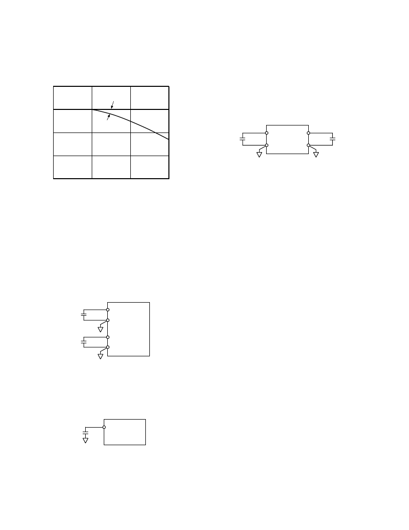
Analog and Digital Supply Decoupling
The AD9240 features separate analog and digital supply and
ground pins, helping to minimize digital corruption of sensitive
analog signals.
FREQUENCY – kHz
120
P
100
1000
80
60
40
100
10
1
AVDD
DVDD
Figure 48. PSRR vs. Frequency
Figure 48 shows the power supply rejection ratio vs. frequency
for a 200 mV p-p ripple applied to both AVDD and DVDD.
In general, AVDD, the analog supply, should be decoupled to
AVSS, the analog common, as close to the chip as physically
possible. Figure 49 shows the recommended decoupling for the
analog supplies; 0.1
μ
F ceramic chip capacitors should provide
adequately low impedance over a wide frequency range. Note
that the AVDD and AVSS pins are co-located on the AD9240
to simplify the layout of the decoupling capacitors and provide
the shortest possible PCB trace lengths. The AD9240/EB power
plane layout, shown in Figure 58, depicts a typical arrangement
using a multilayer PCB.
0.1
m
F
AVDD
AVSS
AD9240
0.1
m
F
AVDD
AVSS
Figure 49. Analog Supply Decoupling
The CML is an internal analog bias point used internally by the
AD9240. This pin must be decoupled with at least a 0.1
μ
F
capacitor as shown in Figure 50. The dc level of CML is ap-
proximately AVDD/2. This voltage should be buffered if it is to
be used for any external biasing.
0.1
m
F
CML
AD9240
Figure 50. CML Decoupling
The digital activity on the AD9240 chip falls into two general
categories: correction logic and output drivers. The internal
correction logic draws relatively small surges of current, mainly
during the clock transitions. The output drivers draw large
current impulses while the output bits are changing. The size
and duration of these currents are a function of the load on the
output bits: large capacitive loads are to be avoided. Note that the
internal correction logic of the AD9240 is referenced DVDD
while the output drivers are referenced to DRVDD.
The decoupling shown in Figure 51, a 0.1
μ
F ceramic chip
capacitor, is appropriate for a reasonable capacitive load on the
digital outputs (typically 20 pF on each pin). Applications
involving greater digital loads should consider increasing the
digital decoupling proportionally and/or using external buffers/
latches.
0.1
m
F
DVDD
DVSS
AD9240
DRVDD
DRVSS
0.1
m
F
Figure 51. Digital Supply Decoupling
A complete decoupling scheme will also include large tantalum
or electrolytic capacitors on the PCB to reduce low-frequency
ripple to negligible levels. For more information regarding the
placement of decoupling capacitors, refer to the AD9240/EB
schematic and layouts in
Figures 54–58.
APPLICATIONS
Direct IF Down Conversion Using the AD9240
Sampling IF signals above an ADC’s baseband region (i.e., dc
to F
S
/2) is becoming increasingly popular in communication
applications. This process is often referred to as Direct IF Down
Conversion or Undersampling. There are several potential benefits
in using the ADC to alias (or mix) down a narrowband or wide-
band IF signal. First and foremost is the elimination of a
complete mixer stage with its associated amplifiers and filters
reducing cost and power dissipation. Second is the ability to
apply various DSP techniques to perform such functions as
filtering, channel selection, quadrature demodulation, data
reduction, detection, etc. A detailed discussion on using this
technique in digital receivers can be found in Analog Devices
Application Notes AN-301 and AN-302.
In Direct IF Down Conversion applications, one exploits the
inherent sampling process of an ADC in which an IF signal
lying outside the baseband region can be aliased back into the
baseband region in a similar manner that a mixer will downconvert
an IF signal. Similar to the mixer topology, an image rejection
filter is required to limit other potential interfering signals from
also aliasing back into the ADC’s baseband region. A tradeoff
exists between the complexity of this image rejection filter and
the sample rate as well as dynamic range of the ADC.
Until recently, the actual implementation of Direct IF Down
Conversion has been limited by the lack of cost-effective ADCs
with sufficiently wide dynamic range and high sample rates for
IFs beyond 10.7 MHz. Since the performance of the AD9240
in the differential mode of operation extends well beyond its
baseband region, it may be well suited as a mix-down converter
in narrowband as well as some wideband applications. Also,
with the full-power bandwidth of the AD9240 extending beyond
60 MHz, various IF frequencies exist over this frequency range
in which the AD9240 maintains excellent dynamic performance.
Figure 52 shows the AD9240 configured in an IF sampling
application at 37.5 MHz. To reduce the complexity of the
digital demodulator in many quadrature demodulation applica-
tions, the IF frequency and/or sample rate are selected such that
相關(guān)PDF資料 |
PDF描述 |
|---|---|
| AD9240AS | Complete 14-Bit, 10 MSPS Monolithic A/D Converter |
| AD9240EB | Complete 14-Bit, 10 MSPS Monolithic A/D Converter |
| AD9241 | Complete 14-Bit, 1.25 MSPS Monolithic A/D Converter |
| AD9241AS | RES., MF, 2K, 1%, 1/4W |
| AD9241EB | Complete 14-Bit, 1.25 MSPS Monolithic A/D Converter |
相關(guān)代理商/技術(shù)參數(shù) |
參數(shù)描述 |
|---|---|
| AD9240AS | 功能描述:IC ADC 14BIT 10MSPS 44-MQFP RoHS:否 類別:集成電路 (IC) >> 數(shù)據(jù)采集 - 模數(shù)轉(zhuǎn)換器 系列:- 標(biāo)準(zhǔn)包裝:1 系列:- 位數(shù):14 采樣率(每秒):83k 數(shù)據(jù)接口:串行,并聯(lián) 轉(zhuǎn)換器數(shù)目:1 功率耗散(最大):95mW 電壓電源:雙 ± 工作溫度:0°C ~ 70°C 安裝類型:通孔 封裝/外殼:28-DIP(0.600",15.24mm) 供應(yīng)商設(shè)備封裝:28-PDIP 包裝:管件 輸入數(shù)目和類型:1 個(gè)單端,雙極 |
| AD9240ASRL | 功能描述:IC ADC 14BIT 10MSPS 44-MQFP RoHS:否 類別:集成電路 (IC) >> 數(shù)據(jù)采集 - 模數(shù)轉(zhuǎn)換器 系列:- 標(biāo)準(zhǔn)包裝:1 系列:- 位數(shù):14 采樣率(每秒):83k 數(shù)據(jù)接口:串行,并聯(lián) 轉(zhuǎn)換器數(shù)目:1 功率耗散(最大):95mW 電壓電源:雙 ± 工作溫度:0°C ~ 70°C 安裝類型:通孔 封裝/外殼:28-DIP(0.600",15.24mm) 供應(yīng)商設(shè)備封裝:28-PDIP 包裝:管件 輸入數(shù)目和類型:1 個(gè)單端,雙極 |
| AD9240ASZ | 功能描述:IC ADC 14BIT 10MSPS 44-MQFP RoHS:是 類別:集成電路 (IC) >> 數(shù)據(jù)采集 - 模數(shù)轉(zhuǎn)換器 系列:- 標(biāo)準(zhǔn)包裝:1 系列:microPOWER™ 位數(shù):8 采樣率(每秒):1M 數(shù)據(jù)接口:串行,SPI? 轉(zhuǎn)換器數(shù)目:1 功率耗散(最大):- 電壓電源:模擬和數(shù)字 工作溫度:-40°C ~ 125°C 安裝類型:表面貼裝 封裝/外殼:24-VFQFN 裸露焊盤 供應(yīng)商設(shè)備封裝:24-VQFN 裸露焊盤(4x4) 包裝:Digi-Reel® 輸入數(shù)目和類型:8 個(gè)單端,單極 產(chǎn)品目錄頁面:892 (CN2011-ZH PDF) 其它名稱:296-25851-6 |
| AD9240ASZRL | 功能描述:IC ADC 14BIT 10MSPS 44-MQFP TR RoHS:是 類別:集成電路 (IC) >> 數(shù)據(jù)采集 - 模數(shù)轉(zhuǎn)換器 系列:- 標(biāo)準(zhǔn)包裝:1 系列:- 位數(shù):14 采樣率(每秒):83k 數(shù)據(jù)接口:串行,并聯(lián) 轉(zhuǎn)換器數(shù)目:1 功率耗散(最大):95mW 電壓電源:雙 ± 工作溫度:0°C ~ 70°C 安裝類型:通孔 封裝/外殼:28-DIP(0.600",15.24mm) 供應(yīng)商設(shè)備封裝:28-PDIP 包裝:管件 輸入數(shù)目和類型:1 個(gè)單端,雙極 |
| AD9240EB | 制造商:AD 制造商全稱:Analog Devices 功能描述:Complete 14-Bit, 10 MSPS Monolithic A/D Converter |
發(fā)布緊急采購,3分鐘左右您將得到回復(fù)。