- 您現在的位置:買賣IC網 > PDF目錄373963 > AD9445-BB-PCB (Analog Devices, Inc.) 14-Bit, 105/125 MSPS, IF Sampling ADC PDF資料下載
參數資料
| 型號: | AD9445-BB-PCB |
| 廠商: | Analog Devices, Inc. |
| 英文描述: | 14-Bit, 105/125 MSPS, IF Sampling ADC |
| 中文描述: | 14位,一百二十五分之一百○五MSPS的,中頻采樣ADC |
| 文件頁數: | 27/40頁 |
| 文件大小: | 965K |
| 代理商: | AD9445-BB-PCB |
第1頁第2頁第3頁第4頁第5頁第6頁第7頁第8頁第9頁第10頁第11頁第12頁第13頁第14頁第15頁第16頁第17頁第18頁第19頁第20頁第21頁第22頁第23頁第24頁第25頁第26頁當前第27頁第28頁第29頁第30頁第31頁第32頁第33頁第34頁第35頁第36頁第37頁第38頁第39頁第40頁
AD9445
Rev. 0 | Page 27 of 40
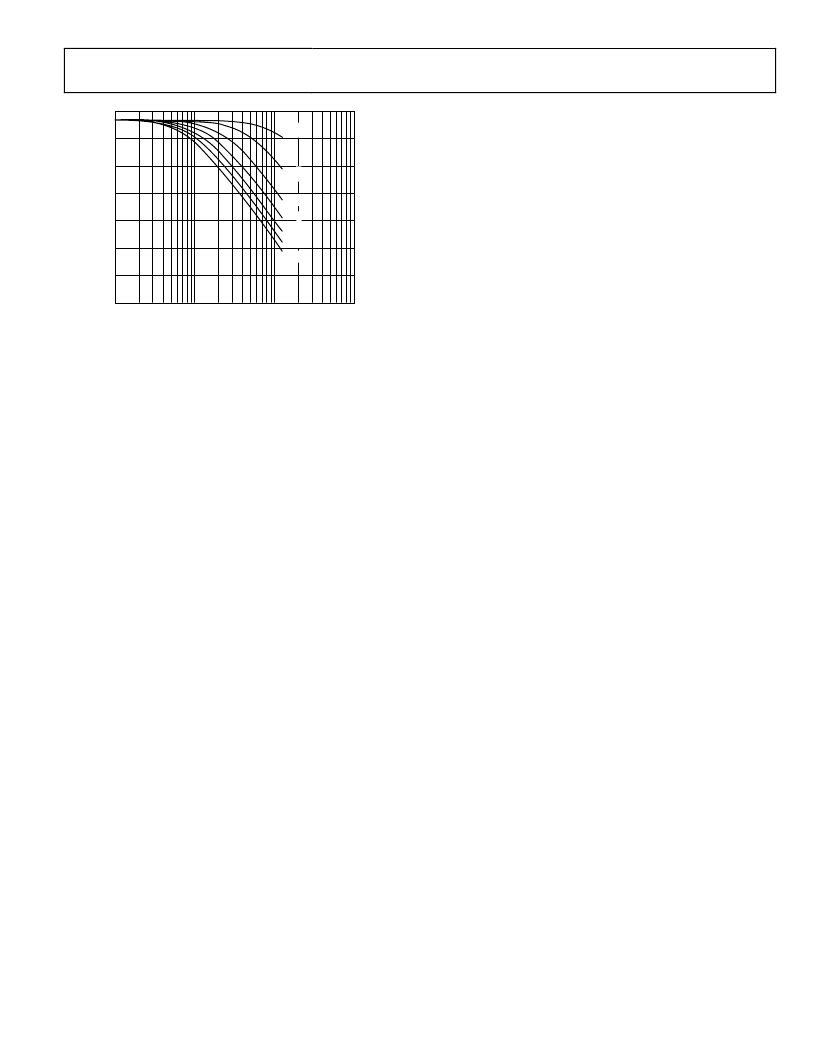
INPUT FREQUENCY (MHz)
S
1
40
75
70
65
60
55
50
45
1000
100
10
0
0.2ps
0.5ps
1.0ps
1.5ps
2.0ps
2.5ps
3.0ps
resistor is placed at Pin 5 (LVDS_BIAS) to ground. Dynamic
performance, including both SFDR and SNR, is maximized
when the AD9445 is used in LVDS mode; designers are
encouraged to take advantage of this mode. The AD9445
outputs include complimentary LVDS outputs for each data bit
(Dx+/Dx), the overrange output (OR+/OR), and the output
data clock output (DCO+/DCO). The R
SET
resistor current is
multiplied on-chip, setting the output current at each output
equal to a nominal 3.5 mA (11 × I
RSET
). A 100 Ω differential
termination resistor placed at the LVDS receiver inputs results
in a nominal 350 mV swing at the receiver. LVDS mode
facilitates interfacing with LVDS receivers in custom ASICs and
FPGAs that have LVDS capability for superior switching
performance in noisy environments. Single point-to-point net
topologies are recommended, with a 100 Ω termination resistor
placed as close to the receiver as possible. It is recommended to
keep the trace length less than 2 inches and to keep differential
output trace lengths as equal as possible.
Figure 66. SNR vs. Input Frequency and Jitter
POWER CONSIDERATIONS
Care should be taken when selecting a power source. The use of
linear dc supplies is highly recommended. Switching supplies
tend to have radiated components that may be received by the
AD9445. Each of the power supply pins should be decoupled as
closely to the package as possible using 0.1 μF chip capacitors.
CMOS Mode
In applications that can tolerate a slight degradation in dynamic
performance, the AD9445 output drivers can be configured to
interface with 2.5 V or 3.3 V logic families by matching
DRVDD to the digital supply of the interfaced logic. CMOS
outputs are available when OUTPUT MODE is CMOS logic
low (or AGND for convenience). In this mode, the output data
bits, Dx, are single-ended CMOS, as is the overrange output,
OR. The output clock is provided as a differential CMOS signal,
DCO+/DCO. Lower supply voltages are recommended to
avoid coupling switching transients back to the sensitive analog
sections of the ADC. The capacitive load to the CMOS outputs
should be minimized, and each output should be connected to a
single gate through a series resistor (220 Ω) to minimize
switching transients caused by the capacitive loading.
The AD9445 has separate digital and analog power supply pins.
The analog supplies are denoted AVDD1 (3.3 V) and AVDD2
(5 V), and the digital supply pins are denoted DRVDD. Although
the AVDD1 and DRVDD supplies can be tied together, best
performance is achieved when the supplies are separate. This is
because the fast digital output swings can couple switching
current back into the analog supplies. Note that both AVDD1
and AVDD2 must be held within 5% of the specified voltage.
The DRVDD supply of the AD9445 is a dedicated supply for the
digital outputs in either LVDS or CMOS output mode. When in
LVDS mode, the DRVDD should be set to 3.3 V. In CMOS
mode, the DRVDD supply can be connected from 2.5 V to
3.6 V for compatibility with the receiving logic.
TIMING
The AD9445 provides latched data outputs with a pipeline delay
of 13 clock cycles. Data outputs are available one propagation
delay (t
PD
) after the rising edge of CLK+. Refer to
Figure 3 for detailed timing diagrams.
DIGITAL OUTPUTS
LVDS Mode
The off-chip drivers on the chip can be configured to provide
LVDS-compatible output levels via Pin 3 (OUTPUT MODE).
LVDS outputs are available when OUTPUT MODE is CMOS
logic high (or AVDD1 for convenience) and a 3.74 kΩ R
SET
Figure 2 and
相關PDF資料 |
PDF描述 |
|---|---|
| AD9445-IF-LVDS | 14-Bit, 105/125 MSPS, IF Sampling ADC |
| AD9446BSVZ-100 | 16-Bit, 80/100 MSPS ADC |
| AD9446BSVZ-80 | 16-Bit, 80/100 MSPS ADC |
| AD9446 | 16-Bit, 80/100 MSPS ADC |
| AD9446-100LVDS | 16-Bit, 80/100 MSPS ADC |
相關代理商/技術參數 |
參數描述 |
|---|---|
| AD9445BSV-105 | 制造商:Analog Devices 功能描述:ADC SGL PIPELINED 105MSPS 14BIT PARALLEL 100TQFP EP - Bulk |
| AD9445BSVZ-105 | 功能描述:IC ADC 14BIT 105MSPS 100-TQFP RoHS:是 類別:集成電路 (IC) >> 數據采集 - 模數轉換器 系列:- 標準包裝:1 系列:- 位數:14 采樣率(每秒):83k 數據接口:串行,并聯 轉換器數目:1 功率耗散(最大):95mW 電壓電源:雙 ± 工作溫度:0°C ~ 70°C 安裝類型:通孔 封裝/外殼:28-DIP(0.600",15.24mm) 供應商設備封裝:28-PDIP 包裝:管件 輸入數目和類型:1 個單端,雙極 |
| AD9445BSVZ-125 | 功能描述:IC ADC 14BIT 125MSPS 100-TQFP RoHS:是 類別:集成電路 (IC) >> 數據采集 - 模數轉換器 系列:- 產品培訓模塊:Lead (SnPb) Finish for COTS Obsolescence Mitigation Program 標準包裝:250 系列:- 位數:12 采樣率(每秒):1.8M 數據接口:并聯 轉換器數目:1 功率耗散(最大):1.82W 電壓電源:模擬和數字 工作溫度:-40°C ~ 85°C 安裝類型:表面貼裝 封裝/外殼:48-LQFP 供應商設備封裝:48-LQFP(7x7) 包裝:管件 輸入數目和類型:2 個單端,單極 |
| AD9445-IF-LVDS | 制造商:AD 制造商全稱:Analog Devices 功能描述:14-Bit, 105/125 MSPS, IF Sampling ADC |
| AD9445-IF-LVDS/PCB | 制造商:Analog Devices 功能描述:Evaluation Kit For 14-Bit, 105/125 MAPA, IF Sampling ADC 制造商:Analog Devices 功能描述:EVAL KIT FOR 14BIT, 105/125 MSPS, IF SAMPLING ADC - Bulk |
發布緊急采購,3分鐘左右您將得到回復。