- 您現在的位置:買賣IC網 > PDF目錄373964 > AD9661A (Analog Devices, Inc.) Laser Diode Driver with Light Power Control(帶光功率控制的激光二極管驅動器) PDF資料下載
參數資料
| 型號: | AD9661A |
| 廠商: | Analog Devices, Inc. |
| 英文描述: | Laser Diode Driver with Light Power Control(帶光功率控制的激光二極管驅動器) |
| 中文描述: | 激光二極管驅動器,帶有光功率控制(帶光功率控制的激光二極管驅動器) |
| 文件頁數: | 8/12頁 |
| 文件大小: | 184K |
| 代理商: | AD9661A |
AD9661A
REV. 0
–8–
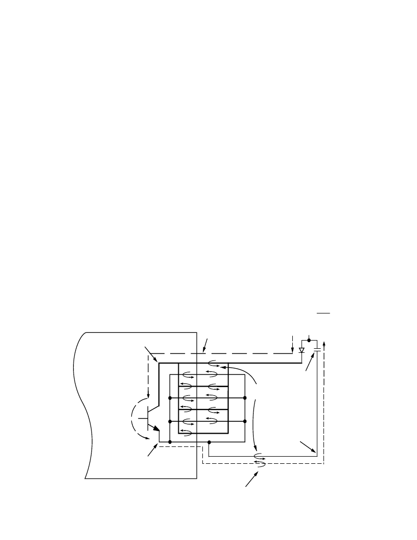
Minimizing the Impedance of the Output Current Path
Because of the very high current slew that the AD9661A is
capable of producing (120+ mA in 1.5 ns), the inductance of
the output current path to and from the laser diode is critical.
A good layout of the output current path will yield high quality
light pulses with rise times of about 1.5 ns and less than 5%
overshoot. A poor layout can result in significant overshoot and
ringing. T he most important guideline for the layout is to mini-
mize the impedance (mostly inductance) of the output current
path to the laser.
It is important to recognize that the laser current path is a
closed loop. T he figure illustrates the path that current travels:
(1) from the +V
S
connection at the anode of the laser to the
cathode (2) from the cathode to the output pins of the
AD9661A (3) through the output drive circuit of the
AD9661A, (4) through the return path (GROUND plane in the
illustration) (5) through the bypass capacitors back to the +V
S
connection of the laser diode. T he inductance of this loop can
be minimized by placing the laser as close to the AD9661A as
possible to keep the loop short, and by placing the send and re-
turn paths on adjacent layers of the PC board to take advantage
of mutual coupling of the path inductances. T his mutual cou-
pling effect is the most important factor in reducing inductance
in the current path.
T he trace from the output pins of the AD9661A to the cathode
of the laser should be several millimeters wide and should be as
direct as possible. T he return current will choose the path of
least resistance. If the return path is the GROUND plane, it
should have an unbroken path, under the output trace, from the
laser anode back to a the AD9661A. If the return path is not
the ground plane (such as on a two layer board, or on the +V
S
plane), it should still be on the board plane adjacent to the
plane of the output trace. If the current cannot return along a
path that follows the output trace, the inductance will be drasti-
cally increased and performance will be degraded.
GROUND PLANE
BYPASS CAPS
GROUND PIN
CONNECTIONS
OUTPUT PIN
CONNECTIONS
PIN ASSIGNMENTS
LASER DIODE CURRENT
PATH SEGMENTS (See Text)
25
24
23
22
21
20
19
MUTUAL COUPLING
REDUCES INDUCTANCE
4
5
2
1
3
AD9661A
26
+V
S
PLANE
Figure 6. Laser Diode Current Loop
Optimizing the Feedback Layout
In applications where the dynamic performance of the analog
feedback loop is important, it is necessary to optimize the layout
of the gain resistor, R
GAIN
, as well as the monitor current path to
SENSE IN. Such applications include systems which recali-
brate the write loop on pulses as short as 25 ns, and closed-loop
applications.
T he best possible T ZA settling will be achieved by using a single
carbon surface mount resistor (usually 5% tolerance) for R
GAIN
and small surface mount capacitor for C
GAIN
. Because the
GAIN pin (Pin 5) is essentially connected to the inverting input
of the T ZA, it is very sensitive to stray capacitance. R
GAIN
should be placed between Pin 5 and Pin 6, as close as possible
to Pin 5. Small traces should be used, and the ground and +V
S
planes adjacent to the trace should be removed to further mini-
mize stray capacitance.
T he trace from SENSE IN to the anode of the PIN photodetec-
tor should be thin and routed away from the laser cathode trace.
E xample Calculations
T he example below (in addition to the one included in the sec-
tions above) should guide users in choosing R
GAIN
, C
GAIN
, the
hold capacitor values, and worst case calibration times.
System Requirements:
Laser power: 4 mW
±
2%
Hold T ime: 0.5 ms
Laser diode/photo diode characteristics:
Laser efficiency 0.3 mW/mA
Monitor current : 0.2 mA/mW
From the laser power requirements and efficiency we can
estimate:
I
OUT MAX
=
4
mW
×
(2.0%)/ 0.3
mW
mA
=
266.6
μ
A
.
相關PDF資料 |
PDF描述 |
|---|---|
| AD9664 | 4-Channel LVDS Dual-Output Laser Diode Driver with Oscillator |
| AD96685 | Ultrafast Comparators |
| AD96685BH | Ultrafast Comparators |
| AD96685BP | Ultrafast Comparators |
| AD96685BQ | Ultrafast Comparators |
相關代理商/技術參數 |
參數描述 |
|---|---|
| AD9661AKR | 制造商:Rochester Electronics LLC 功能描述:DUAL POWER LDD - Bulk 制造商:Analog Devices 功能描述: |
| AD9661AKR-REEL | 制造商:AD 制造商全稱:Analog Devices 功能描述:Laser Diode Driver with Light Power Control |
| AD9662 | 制造商:Analog Devices 功能描述:- Bulk |
| AD9662ARQZ | 制造商:Analog Devices 功能描述:LASER DRVR 3-CH 16QSOP - Rail/Tube |
| AD9662ARQZ-REEL7 | 功能描述:IC LASER DIODE DRIVER 3CH 16QSOP RoHS:是 類別:集成電路 (IC) >> PMIC - 激光驅動器 系列:- 產品培訓模塊:Lead (SnPb) Finish for COTS Obsolescence Mitigation Program 標準包裝:60 系列:- 類型:激光二極管驅動器 數據速率:- 通道數:4 電源電壓:3.3V 電流 - 電源:- 電流 - 調制:- 電流 - 偏置:- 工作溫度:0°C ~ 70°C 封裝/外殼:40-TQFN 裸露焊盤 供應商設備封裝:40-TQFN EP 包裝:托盤 安裝類型:表面貼裝 |
發布緊急采購,3分鐘左右您將得到回復。