- 您現在的位置:買賣IC網 > PDF目錄373968 > AD9826 (Analog Devices, Inc.) Complete 16-Bit Imaging Signal Processor PDF資料下載
參數資料
| 型號: | AD9826 |
| 廠商: | Analog Devices, Inc. |
| 英文描述: | Complete 16-Bit Imaging Signal Processor |
| 中文描述: | 完整的16位影像信號處理器 |
| 文件頁數: | 18/20頁 |
| 文件大小: | 159K |
| 代理商: | AD9826 |
AD9826
–18–
REV. A
TOP VIEW
(Not to Scale)
28
27
26
25
24
23
22
21
20
19
18
17
16
15
1
2
3
4
5
6
7
8
9
10
11
12
13
14
AD9826
CDSCLK1
CDSCLK2
ADCCLK
OEB
DRVDD
DRVSS
(MSB) D7
D6
D5
D4
D3
D2
D1
(LSB)D0
AVDD
AVSS
VINR
OFFSET
VING
CML
VINB
CAPT
CAPB
AVSS
AVDD
SLOAD
SCLK
SDATA
0.1 F
0.1 F
0.1 F
0.1 F
10 F
0.1 F
0.1 F
0.1 F
RED INPUT
GREEN INPUT
BLUE INPUT
CLOCK
INPUTS
0.1 F
DATA
INPUTS
5V/3V
5V
0.1 F
1.0 F
0.1 F
0.1 F
5V
SERIAL
INTERFACE
Figure 18. Recommended Circuit Configuration, 3-Channel CDS Mode
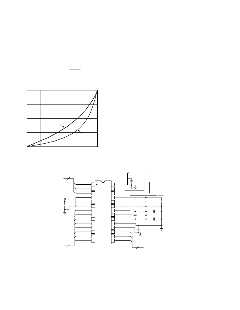
Programmable Gain Amplifiers
T he AD9826 uses one Programmable Gain Amplifier (PGA) for
each channel. Each PGA has a gain range from 1
×
(0 dB) to
6.0
×
(15.56 dB), adjustable in 64 steps. Figure 17 shows the
PGA gain as a function of the PGA register code. Although the
gain curve is approximately “linear in dB,” the gain in V/V var-
ies nonlinearly with register code, following the equation:
Gain
G
=
6 0
.
1 5 0
63
63
.
–
where
G
is the decimal value of the gain register contents, and
varies from 0 to 63.
PGA REGISTER VALUE
–
Decimal
00
12
G
–
4
12
24
36
63
GAIN
–
V/V
GAIN
–
dB
G
–
48
60
8
16
1.00
2.25
4.75
3.50
6.00
Figure 17. PGA Gain Transfer Function
APPLICAT IONS INFORMAT ION
Circuit and Layout Recommendations
T he recommended circuit configuration for 3-Channel CDS
Mode operation is shown in Figure 18. T he recommended
input coupling capacitor value is 0.1
μ
F (see Circuit Operation
section for more details). A single ground plane is recommended
for the AD9826. A separate power supply may be used for
DRVDD, the digital driver supply, but this supply pin should
still be decoupled to the same ground plane as the rest of the
AD9826. T he loading of the digital outputs should be mini-
mized, either by using short traces to the digital ASIC, or by
using external digital buffers. T o minimize the effect of digital
transients during major output code transitions, the falling edge
of CDSC L K 2 should occur coincident with or before the
rising edge of ADCCLK (see Figures 1 through 6 for timing).
All 0.1
μ
F decoupling capacitors should be located as close as
possible to the AD9826 pins. When operating in 1CH or 2CH
Mode, the unused analog inputs should be grounded.
For 3-Channel SHA Mode, all of the above considerations also
apply, except that the analog input signals are directly connected
to the AD9826 without the use of coupling capacitors. T he analog
input signals must already be dc-biased between 0 V and 4 V.
Also, the OFFSET pin should be grounded if the inputs to the
AD9826 are to be referenced to ground, or a dc offset voltage
should be applied to the OFFSET pin in the case where a coarse
offset needs to be removed from the inputs. (See Figure 16 and
the Circuit Operation section for more details.)
相關PDF資料 |
PDF描述 |
|---|---|
| AD9830 | CMOS Complete DDS |
| AD9830AST | CMOS Complete DDS |
| AD9831 | CMOS Complete DDS |
| AD9831AST | CMOS Complete DDS |
| AD9832 | CMOS Complete DDS |
相關代理商/技術參數 |
參數描述 |
|---|---|
| AD9826_12 | 制造商:AD 制造商全稱:Analog Devices 功能描述:Complete 16-Bit Imaging Signal Processor |
| AD9826-EB | 制造商:Analog Devices 功能描述:- Bulk |
| AD9826KRS | 制造商:Analog Devices 功能描述:AFE Video 1ADC 16-Bit 5V 28-Pin SSOP Tube 制造商:Analog Devices 功能描述:IC 16-BIT SIGNAL PROCESSOR |
| AD9826KRSRL | 制造商:Analog Devices 功能描述:AFE Video 1ADC 16-Bit 5V 28-Pin SSOP T/R |
| AD9826KRSZ | 功能描述:IC IMAGE SGNL PROC 16BIT 28-SSOP RoHS:是 類別:集成電路 (IC) >> 接口 - 傳感器和探測器接口 系列:- 其它有關文件:Automotive Product Guide 產品培訓模塊:Lead (SnPb) Finish for COTS Obsolescence Mitigation Program 標準包裝:74 系列:- 類型:觸控式傳感器 輸入類型:數字 輸出類型:數字 接口:JTAG,串行 電流 - 電源:100µA 安裝類型:表面貼裝 封裝/外殼:20-TSSOP(0.173",4.40mm 寬) 供應商設備封裝:20-TSSOP 包裝:管件 |
發布緊急采購,3分鐘左右您將得到回復。