- 您現(xiàn)在的位置:買賣IC網(wǎng) > PDF目錄373969 > AD9870EB (Analog Devices, Inc.) IF Digitizing Subsystem PDF資料下載
參數(shù)資料
| 型號(hào): | AD9870EB |
| 廠商: | Analog Devices, Inc. |
| 英文描述: | IF Digitizing Subsystem |
| 中文描述: | 中頻數(shù)字化子系統(tǒng) |
| 文件頁數(shù): | 1/20頁 |
| 文件大小: | 233K |
| 代理商: | AD9870EB |
REV. 0
Information furnished by Analog Devices is believed to be accurate and
reliable. However, no responsibility is assumed by Analog Devices for its
use, nor for any infringements of patents or other rights of third parties that
may result from its use. No license is granted by implication or otherwise
under any patent or patent rights of Analog Devices.
a
AD9870
One Technology Way, P.O. Box 9106, Norwood, MA 02062-9106, U.S.A.
Tel: 781/329-4700
Fax: 781/326-8703
www.analog.com
Analog Devices, Inc., 2001
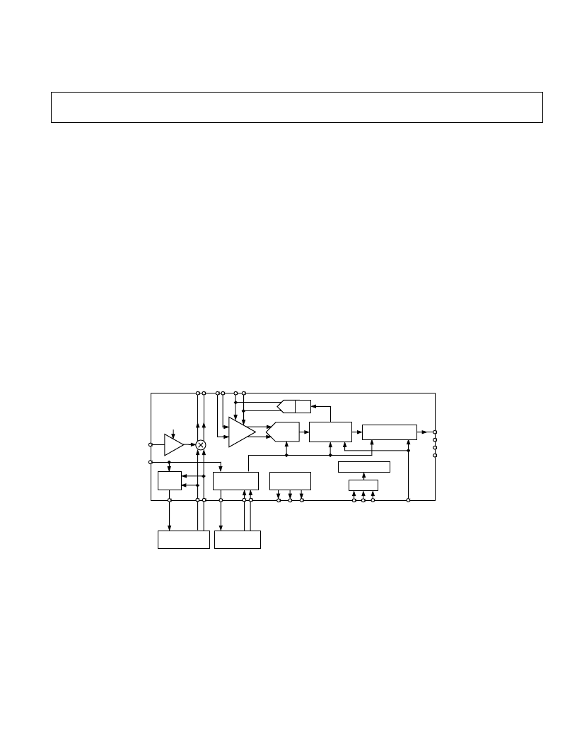
IF Digitizing Subsystem
FUNCTIONAL BLOCK DIAGRAM
IFIN
FREF
AD9870
LNA
–16dB
LO
SYNTH
I
L
L
I
C
C
V
V
V
P
P
P
S
LO VCO AND
LOOP FILTER
CLK VCO AND
LOOP FILTER
SAMP CLOCK
SYNTHESIZER
M
M
I
I
G
G
DECIMATION
FILTER
CONTROL LOGIC
f
CLK
= 18MHz
- ADC
DAC AGC
SPI
VOLTAGE
REFERENCE
FORMATTING/SSI
DOUTA
DOUTB
FS
CLKOUT
VGA/
AAF
FEATURES
10 MHz–300 MHz Input Frequency
Baseband (I/Q) Digital Output
10 kHz–150 kHz Output Signal Bandwidth
12 dB SSB NF
> –1 dBm IIP3 (High IIP3 Mode)
25 dB Continuous AGC Range + 16 dB Gain Step
Support for LO and Sampling Clock Synthesis
Programmable Decimation Rate, Output Format, AAF
Cutoff, AGC and Synthesizer Settings
360
Input Impedance
2.7 V–3.6 V Supply Voltage
Low Current: 42 mA Typ (High IIP3 Mode),
30 mA Typ (Low IIP3, Fixed Gain Mode)
48-Lead LQFP Package (1.4 mm Thick)
APPLICATIONS
Portable and Mobile Radio Products
Digital UHF/VHF FDMA Products
TETRA
PRODUCT DESCRIPTION
The AD9870 is a general-purpose IF subsystem that digitizes a
low-level 10 MHz–300 MHz IF input with a bandwidth of up to
150 kHz. The signal chain of the AD9870 consists of a low-noise
amplifier, a mixer, a variable gain amplifier with integral antialias
filter, a bandpass sigma-delta analog-to-digital converter, and a
decimation filter with programmable decimation factor. An auto-
matic gain control (AGC) circuit provides the AD9870 with
25 dB of continuous gain adjustment. The high dynamic range
of the bandpass sigma-delta converter allows the AD9870 to
cope with blocking signals that are as much as 70 dB stronger
than the desired signal. Auxiliary blocks include clock and LO
synthesizers as well as a serial peripheral interface (SPI) port.
The SPI port programs numerous parameters of the AD9870,
including the synthesizer divide ratios, the AGC attack and decay
times, the AGC target signal level, the decimation factor, the
output data format, the 16 dB attenuator, and the bias currents of
several blocks. Reducing bias currents allows the user to reduce
power consumption at the expense of reduced performance.
相關(guān)PDF資料 |
PDF描述 |
|---|---|
| AD9873 | Analog Front End Converter for Set-Top Box, Cable Modem |
| AD9873-EB | Analog Front End Converter for Set-Top Box, Cable Modem |
| AD9873JS | Analog Front End Converter for Set-Top Box, Cable Modem |
| AD9874 | IF Digitizing Subsystem |
| AD9874BST | IF Digitizing Subsystem |
相關(guān)代理商/技術(shù)參數(shù) |
參數(shù)描述 |
|---|---|
| AD9873 | 制造商:AD 制造商全稱:Analog Devices 功能描述:Analog Front End Converter for Set-Top Box, Cable Modem |
| AD9873-EB | 制造商:Analog Devices 功能描述: |
| AD9873JS | 制造商:Analog Devices 功能描述: |
| AD9874 | 制造商:AD 制造商全稱:Analog Devices 功能描述:IF Digitizing Subsystem |
| AD9874ABST | 功能描述:IC IF DIGIT SUBSYSTEM 48-LQFP RoHS:否 類別:RF/IF 和 RFID >> RF 其它 IC 和模塊 系列:- 標(biāo)準(zhǔn)包裝:100 系列:* |
發(fā)布緊急采購,3分鐘左右您將得到回復(fù)。