- 您現在的位置:買賣IC網 > PDF目錄373969 > AD9873 (Analog Devices, Inc.) Analog Front End Converter for Set-Top Box, Cable Modem PDF資料下載
參數資料
| 型號: | AD9873 |
| 廠商: | Analog Devices, Inc. |
| 英文描述: | Analog Front End Converter for Set-Top Box, Cable Modem |
| 中文描述: | 模擬前端轉換器,用于機頂盒,電纜調制解調器 |
| 文件頁數: | 23/39頁 |
| 文件大小: | 935K |
| 代理商: | AD9873 |
第1頁第2頁第3頁第4頁第5頁第6頁第7頁第8頁第9頁第10頁第11頁第12頁第13頁第14頁第15頁第16頁第17頁第18頁第19頁第20頁第21頁第22頁當前第23頁第24頁第25頁第26頁第27頁第28頁第29頁第30頁第31頁第32頁第33頁第34頁第35頁第36頁第37頁第38頁第39頁
REV. 0
AD9873
–23–
PROGRAMMABLE CLOCK OUTPUT REF CLK
The AD9873 provides a frequency programmable clock output
REF CLK (Pin 71). MCLK (f
MCLK
) and the master clock divider
ratio R stored in register address 01h determine its frequency:
f
REF CLK
=
f
MCLK
/
R
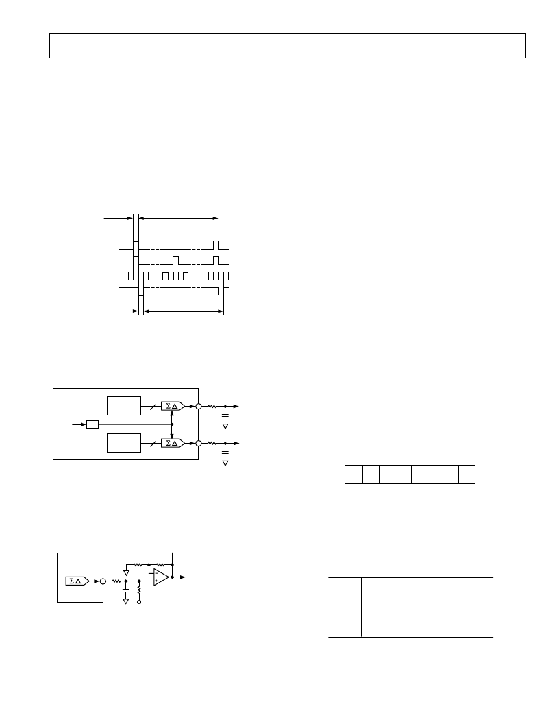
SIGMA-DELTA OUTPUTS
The AD9873 contains two independent sigma-delta outputs
that when low-pass filtered generate level programmable DC
voltages of:
V
SD
= (
Sigma
-
Delta Code
)/4096)(
V
LOGIC1
) +
V
LOGIC0
(Influenced by CMOS logic output levels.)
8
t
MCLK
000h
001h
002h
800h
FFFh
8
t
MCLK
4096 8
t
MCLK
4096 8
t
MCLK
Figure 3. Sigma-Delta Output Signals
In cable modem set-top box applications the outputs can be used
to control external variable gain amplifiers and RF tuners. A
simple single-pole R-C low-pass filter provides sufficient filtering
(see Figure 4).
12
12
8
SIGMA-DELTA 1
SIGMA-DELTA 0
CONTROL
WORD 1
CONTROL
WORD 0
MCLK
R
R
C
C
DC (0.4 TO
DRVDD-0.6V)
DC (0.4 TO
DRVDD-0.6V)
TYPICAL: R = 50k
C = 0.01 F
f
–
3dB
= 1/(2 RC) = 318Hz
AD9873
Figure 4. Sigma-Delta RC Filter
In more demanding applications where additional gain, level-shift
or drive capability is required, a first
or second order active filter
might be considered for each sigma-delta output (see Figure 5).
SIGMA-DELTA
R
C
V
= (V
/2 + V
) (1 + R/R1)
GAIN = (1 + R/R1)/2
V
OFFSET
= V
OFFSETREF
(1 + R/R1)
TYPICAL: R = 50k
C = 0.01 F
f
–
3dB
= 1/(2 RC) = 318Hz
AD9873
R
V
OFFSETREF
OP250
R1
R
C
Figure 5. Sigma-Delta Active Filter With Gain and Offset
SERIAL INTERFACE FOR REGISTER CONTROL
The AD9873 serial port is a flexible, synchronous serial communi-
cations port allowing easy interface to many industry standard
microcontrollers and microprocessors. The serial I/O is com-
patible with most synchronous transfer formats, including both the
Motorola SPI and Intel SSR protocols. The interface allows read/
write access to all registers that configure the AD9873. Single
or multiple byte transfers are supported as well as MSB first or
LSB first transfer formats. The AD9873’s serial interface port can
be configured as a single pin I/O (SDIO) or two unidirectional pins
for in/out (SDIO/SDO).
General Operation of the Serial Interface
There are two phases to a communication cycle with the AD9873.
Phase 1 is the instruction cycle, which is the writing of an instruc-
tion byte into the AD9873, coincident with the first eight SCLK
rising edges. The instruction byte provides the AD9873 serial port
controller with information regarding the data transfer cycle, which
is Phase 2 of the communication cycle. The Phase 1 instruction
byte defines whether the upcoming data transfer is read or write,
the number of bytes in the data transfer and the starting register
address for the first byte of the data transfer. The first eight SCLK
rising edges of each communication cycle are used to write the
instruction byte into the AD9873.
The remaining SCLK edges are for Phase 2 of the communication
cycle. Phase 2 is the actual data transfer between the AD9873 and
the system controller. Phase 2 of the communication cycle is
a transfer of 1, 2, 3, or 4 data bytes as determined by the
instruction byte. Normally, using one multibyte transfer is
the preferred method. However, single byte data transfers are
useful to reduce CPU overhead when register access requires
one byte only. Registers change
immediately
upon writing to the
last bit of each transfer byte.
Instruction Byte
The instruction byte contains the following information as shown
in Table II:
Table II. Instruction Byte Information
I7
I6
N1
I5
N0
I4
A4
I3
A3
I2
A2
I1
A1
I0
A0
R/W
MSB
LSB
R/W, Bit 7 of the instruction byte, determines whether a read or
a write data transfer will occur after the instruction byte write.
Logic high indicates read operation. Logic zero indicates a write
operation. N1, N0, Bits 6 and 5 of the instruction byte, determine
the number of bytes to be transferred during the data transfer
cycle. The bit decodes are shown in the Table III.
Table III. Decode Bits
N1
N0
Description
0
0
1
1
0
1
0
1
Transfer 1 Byte
Transfer 2 Bytes
Transfer 3 Bytes
Transfer 4 Bytes
A4, A3, A2, A1, A0, Bits 4, 3, 2, 1, 0, of the instruction byte,
determine which register is accessed during the data transfer
portion of the communications cycle. For multibyte transfers,
this address is the starting byte address. The remaining register
addresses are generated by the AD9873.
相關PDF資料 |
PDF描述 |
|---|---|
| AD9873-EB | Analog Front End Converter for Set-Top Box, Cable Modem |
| AD9873JS | Analog Front End Converter for Set-Top Box, Cable Modem |
| AD9874 | IF Digitizing Subsystem |
| AD9874BST | IF Digitizing Subsystem |
| AD9874EB | IF Digitizing Subsystem |
相關代理商/技術參數 |
參數描述 |
|---|---|
| AD9873-EB | 制造商:Analog Devices 功能描述: |
| AD9873JS | 制造商:Analog Devices 功能描述: |
| AD9874 | 制造商:AD 制造商全稱:Analog Devices 功能描述:IF Digitizing Subsystem |
| AD9874ABST | 功能描述:IC IF DIGIT SUBSYSTEM 48-LQFP RoHS:否 類別:RF/IF 和 RFID >> RF 其它 IC 和模塊 系列:- 標準包裝:100 系列:* |
| AD9874ABST | 制造商:Analog Devices 功能描述:IF DIGITIZING SYBSYSTEM ((NW)) 制造商:Analog Devices 功能描述:IC, IF DIGITIZING SUBSYSTEM, LQFP-48 |
發布緊急采購,3分鐘左右您將得到回復。