- 您現在的位置:買賣IC網 > PDF目錄373969 > AD9874EB (Analog Devices, Inc.) IF Digitizing Subsystem PDF資料下載
參數資料
| 型號: | AD9874EB |
| 廠商: | Analog Devices, Inc. |
| 英文描述: | IF Digitizing Subsystem |
| 中文描述: | 中頻數字化子系統 |
| 文件頁數: | 1/40頁 |
| 文件大小: | 744K |
| 代理商: | AD9874EB |
當前第1頁第2頁第3頁第4頁第5頁第6頁第7頁第8頁第9頁第10頁第11頁第12頁第13頁第14頁第15頁第16頁第17頁第18頁第19頁第20頁第21頁第22頁第23頁第24頁第25頁第26頁第27頁第28頁第29頁第30頁第31頁第32頁第33頁第34頁第35頁第36頁第37頁第38頁第39頁第40頁
REV. 0
a
Information furnished by Analog Devices is believed to be accurate and
reliable. However, no responsibility is assumed by Analog Devices for its
use, nor for any infringements of patents or other rights of third parties that
may result from its use. No license is granted by implication or otherwise
under any patent or patent rights of Analog Devices.
Tel: 781/329-4700Fax: 781/326-8703
Analog Devices, Inc., 2002AD9874
*
IF Digitizing Subsystem
*
Protected by U.S. Patent No. 5,969,657; other patents pending.
FEATURES
10 MHz–300 MHz Input Frequency
6.8 kHz–270 kHz Output Signal Bandwidth
8.1 dB SSB NF
0 dBm IIP3
AGC Free Range up to –34 dBm
12 dB Continuous AGC Range
16 dB Front End Attenuator
Baseband I/Q 16-bit (or 24-bit) Serial Digital Output
LO and Sampling Clock Synthesizers
Programmable Decimation Factor, Output Format,
AGC, and Synthesizer Settings
370
Input Impedance
2.7 V–3.6 V Supply Voltage
Low Current Consumption: 20 mA
48–Lead LQFP Package (1.4 mm Thick)
APPLICATIONS
Multimode Narrowband Radio Products
Analog/Digital UHF/VHF FDMA Receivers
TETRA, APCO25, GSM/EDGE
Portable and Mobile Radio Products
Base Station Applications
GENERAL DESCRIPTION
The AD9874 is a general-purpose IF subsystem that digitizes a
low level 10 MHz–300 MHz IF input with a signal bandwidth
ranging from 6.8 kHz to 270 kHz. The signal chain of the AD9874
consists of a low noise amplifier, a mixer, a band-pass sigma-delta
analog-to-digital converter, and a decimation filter with program-
mable decimation factor. An automatic gain control (AGC) circuit
gives the AD9874 12 dB of continuous gain adjustment. Auxiliary
blocks include both clock and LO synthesizers.
The AD9874’s high dynamic range and inherent antialiasing
provided by the band-pass sigma-delta converter allow the
AD9874
to cope with blocking signals up to 95 dB stronger
than the desired signal. This attribute can often reduce the cost of
a
radio by reducing its IF filtering requirements. Also, it enables
multimode radios of varying channel bandwidths, allowing the
IF filter to be specified for the largest channel bandwidth.
The SPI port programs numerous parameters of the AD9874,
thus allowing the device to be optimized for any given
application. Programmable parameters include the following:
synthesizer divide ratios; AGC attenuation and attack/decay
time; the received signal strength level; decimation factor; the
output data format; 16 dB attenuator; and the selected bias
currents. The bias currents of the LNA and mixer can be further
reduced at the expense of the degraded performance for battery-
powered applications.
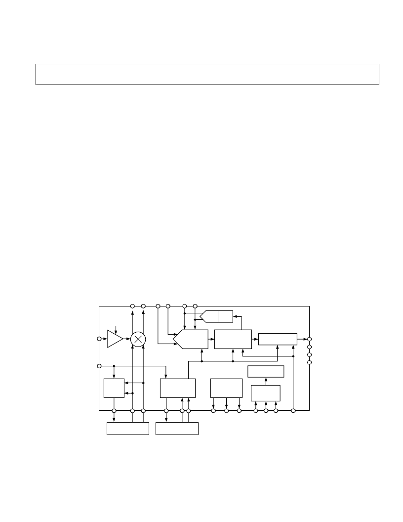
FUNCTIONAL BLOCK DIAGRAM
MXOP MXON IF2P IF2N
GCP GCN
- ADC
LNA
DAC
AGC
VOLTAGE
REFERENCE
SPI
CONTROL LOGIC
FORMATTING/SSI
DECIMATION
FILTER
LO
SYNC
SAMPLE CLOCK
SYNTHESIZER
LO VCO AND
LOOP FILTER
IFIN
FREF
DOUTA
DOUTB
FS
CLKOUT
SYNCB
PE
PD
PC
VREFN
VCM
VREFP
–16dB
AD9874
CLKN
CLKP
IOUTC
LON
LOP
IOUTL
LO VCO AND
LOOP FILTER
相關PDF資料 |
PDF描述 |
|---|---|
| AD9875BSTRL | Broadband Modem Mixed-Signal Front End |
| AD9875 | Broadband Modem Mixed-Signal Front End |
| AD9875-EB | Broadband Modem Mixed-Signal Front End |
| AD9875BST | Broadband Modem Mixed-Signal Front End |
| AD9876 | Broadband Modem Mixed-Signal Front End |
相關代理商/技術參數 |
參數描述 |
|---|---|
| AD9874-EB | 制造商:Analog Devices 功能描述: |
| AD9874-EBZ | 功能描述:BOARD EVAL FOR AD9874 制造商:analog devices inc. 系列:- 零件狀態:有效 類型:數字轉換器 頻率:10MHz ~ 300MHz 配套使用產品/相關產品:AD9874 所含物品:板 標準包裝:1 |
| AD9875 | 制造商:AD 制造商全稱:Analog Devices 功能描述:Broadband Modem Mixed-Signal Front End |
| AD9875BST | 制造商:Analog Devices 功能描述:Modem Chip Single 48-Pin LQFP 制造商:Rochester Electronics LLC 功能描述:10B BROADBAND MODEM MXFE CONVERTER - Tape and Reel |
| AD9875BSTRL | 制造商:Analog Devices 功能描述:Modem Chip Single 48-Pin LQFP T/R |
發布緊急采購,3分鐘左右您將得到回復。