- 您現在的位置:買賣IC網 > PDF目錄373969 > AD9874EB (Analog Devices, Inc.) IF Digitizing Subsystem PDF資料下載
參數資料
| 型號: | AD9874EB |
| 廠商: | Analog Devices, Inc. |
| 英文描述: | IF Digitizing Subsystem |
| 中文描述: | 中頻數字化子系統 |
| 文件頁數: | 29/40頁 |
| 文件大小: | 744K |
| 代理商: | AD9874EB |
第1頁第2頁第3頁第4頁第5頁第6頁第7頁第8頁第9頁第10頁第11頁第12頁第13頁第14頁第15頁第16頁第17頁第18頁第19頁第20頁第21頁第22頁第23頁第24頁第25頁第26頁第27頁第28頁當前第29頁第30頁第31頁第32頁第33頁第34頁第35頁第36頁第37頁第38頁第39頁第40頁
REV. 0
AD9874
–29–
the maximum bandwidth is 9 kHz. A general expression for the
attack bandwidth is:
BW
and the corresponding attack time is:
assuming that the loop dynamics are essentially those of a
single-pole system.
The 4-bit code in the AGCD field sets the ratio of the attack
time to the decay time in the amplitude estimation circuitry. When
AGCD is zero, this ratio is one. Incrementing AGCD multiplies
the decay time constant by 2
1/2
, allowing a 180:1 range in the
decay time relative to the attack time. The decay time may be
computed from:
(
2
f
MHz
Hz
A
CLK
AGCA
=
×
(
)
×
(
)
50
18
2
2
(8)
tattack
BW
AGCA
A
=
×
×
=
(
)
2 2
.
100
2
0 35
.
2
π
(9)
tdecay
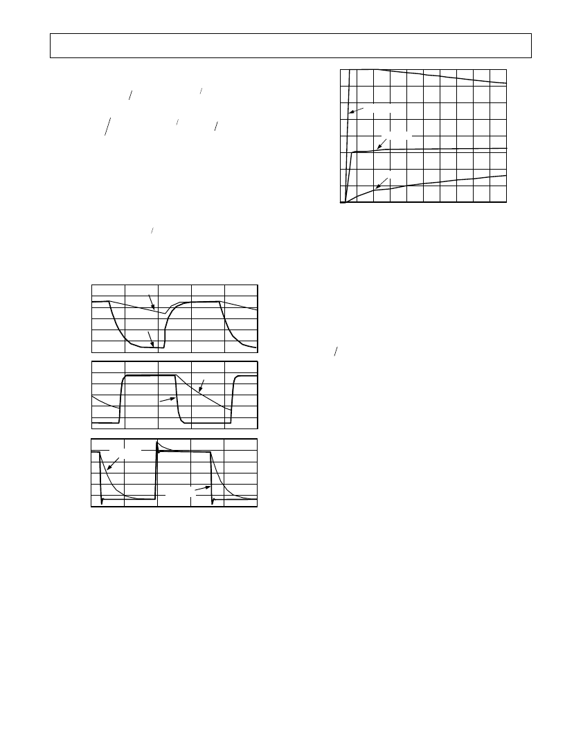
Figure 21a shows the AGC response to a 30 Hz pulse-modulated
IF burst for different AGCA and AGCD settings.
tattack
AGCD
=
×
)
2
(10)
AGCA = 0
80
64
0
96
48
32
16
96
TIME – ms
10
20
0
50
40
30
80
64
0
48
32
16
96
V
AGCA = 4
80
64
0
48
32
16
AGCA = 8
AGCD = 8
AGCD = 0
AGCD = 8
AGCD = 0
AGCD = 8
AGCD = 0
Figure 21a. AGC Response for Different AGCA and AGCD
Settings with f
CLK
= 18 MSPS, f
CLKOUT
= 20 kSPS, Deci-
mate by 900, and AGCO = 0
The 3-bit value in the AGCO field determines the amount of
attenuation added in response to a reset event in the ADC.
Each increment in AGCO doubles the weighting factor. At the
highest AGCO setting, the attenuation will change from 0 dB to
12 dB in approximately 10
μ
s, while at the lowest setting the
attenuation will change from 0 dB to 12 dB in approximately
1.2 ms. Both times assume
f
CLK
= 18 MHz. Figure 21b shows
the AGC attack time response for different AGCO settings.
V
TIME – msec
0.1
0.2
0
0.5
0.4
0.3
80
64
0
48
32
16
96
1.0
0.9
0.8
0.7
0.6
112
128
AGCO = 7
AGCO = 4
AGCD = 0
Figure 21b. AGC Response for Different AGCO Settings
with f
CLK
= 18 MSPS, f
CLKOUT
= 300 kSPS, Decimate by 60, and
AGCA = AGCD = 0
Lastly, the AGCF bit reduces the DAC source resistance by at
least a factor of 10. This facilitates fast acquisition by lowering
the RC time constant that is formed with the external capacitors
connected from the GCP pin-to-ground (GCN Pin). For an
overshoot-free step response in the AGC loop, the capacitor
connected from the GCP pin to the GCN ground pin should be
chosen so that the RC time constant is less than one quarter
that of the raw loop. Specifically:
RC
where
R
is the resistance between the GCP Pin and ground (64kW
±
20% if AGCF = 0, < 7 kW if AGCF = 1) and
BW
is the raw
loop bandwidth. Note that with
C
chosen at this upper limit, the
loop bandwidth increases by approximately 30%.
Now consider the same case as above but with the DVGA enabled
to minimize the effects of 16-bit truncation. With the DVGA
enabled, a control loop based on the larger of the two estimated
signal levels (i.e., output of DEC1 and DVGA) is used to control
the DVGA gain. The DVGA multiplies the output of the deci-
mation filter by a factor ranging from 1 to 4 (i.e., 0 dB to 12 dB).
When signals are small, the DVGA gain is 4 and the 16-bit output
is extracted from the 24-bit data produced by the decimation
filter by dropping 2 MSBs and taking the next 16-bits. As signals
get larger, the DVGA gain decreases until the point where the
DVGA gain is 1 and the 16-bit output data is simply the 16 MSBs
of the internal 24-bit data. As signals get even larger, attenuation
is accomplished by the normal method of increasing the ADC’s
full scale.
The extra 12 dB of gain range provided by the DVGA reduces
the input-referred truncation noise by 12 dB and makes the data
more tolerant of LSB corruption within the DSP. The price
paid for this extension to the gain range is that the start of AGC
action is 12 dB lower and that the AGC loop will be unstable if
its bandwidth is set too wide. The latter difficulty results from
the large delay of the decimation filters, DEC2 and DEC3,
when one implements a large decimation factor. As a result, given
an option, the use of 24-bit data is preferable to using the DVGA.
BW
π
<
1 8
(
)
(11)
相關PDF資料 |
PDF描述 |
|---|---|
| AD9875BSTRL | Broadband Modem Mixed-Signal Front End |
| AD9875 | Broadband Modem Mixed-Signal Front End |
| AD9875-EB | Broadband Modem Mixed-Signal Front End |
| AD9875BST | Broadband Modem Mixed-Signal Front End |
| AD9876 | Broadband Modem Mixed-Signal Front End |
相關代理商/技術參數 |
參數描述 |
|---|---|
| AD9874-EB | 制造商:Analog Devices 功能描述: |
| AD9874-EBZ | 功能描述:BOARD EVAL FOR AD9874 制造商:analog devices inc. 系列:- 零件狀態:有效 類型:數字轉換器 頻率:10MHz ~ 300MHz 配套使用產品/相關產品:AD9874 所含物品:板 標準包裝:1 |
| AD9875 | 制造商:AD 制造商全稱:Analog Devices 功能描述:Broadband Modem Mixed-Signal Front End |
| AD9875BST | 制造商:Analog Devices 功能描述:Modem Chip Single 48-Pin LQFP 制造商:Rochester Electronics LLC 功能描述:10B BROADBAND MODEM MXFE CONVERTER - Tape and Reel |
| AD9875BSTRL | 制造商:Analog Devices 功能描述:Modem Chip Single 48-Pin LQFP T/R |
發布緊急采購,3分鐘左右您將得到回復。