- 您現在的位置:買賣IC網 > PDF目錄373969 > AD9874EB (Analog Devices, Inc.) IF Digitizing Subsystem PDF資料下載
參數資料
| 型號: | AD9874EB |
| 廠商: | Analog Devices, Inc. |
| 英文描述: | IF Digitizing Subsystem |
| 中文描述: | 中頻數字化子系統 |
| 文件頁數: | 32/40頁 |
| 文件大小: | 744K |
| 代理商: | AD9874EB |
第1頁第2頁第3頁第4頁第5頁第6頁第7頁第8頁第9頁第10頁第11頁第12頁第13頁第14頁第15頁第16頁第17頁第18頁第19頁第20頁第21頁第22頁第23頁第24頁第25頁第26頁第27頁第28頁第29頁第30頁第31頁當前第32頁第33頁第34頁第35頁第36頁第37頁第38頁第39頁第40頁
REV. 0
–32–
AD9874
Many applications have frequency plans that take advantage of
industry-standard IF frequencies due to the large selection of
low cost crystal or SAW filters. If the selected IF frequency and
ADC clock rate result in a problematic spurious component, an
alternative ADC clock rate should be selected by slightly modi-
fying the decimation factor and CLK synthesizer settings (if
used) such that the output sample rate remains the same. Also,
applications requiring a certain degree of tuning range should
take into consideration the location and magnitude of these spurs
when determining the tuning range as well as optimum IF and
ADC clock frequency.
Figure 23a plots the measured in-band noise power as a function of
the LO frequency for f
CLK
= 18 MHz and an output signal band-
width of 150 kHz when no signal is present. Any LO frequency
resulting in large spurs should be avoided. As this figure shows,
large spurs result when the LO is f
CLK
/8 = 2.25 MHz away from a
harmonic of 18 MHz (i.e.,
n f
CLK
f
CLK
/8). Also problematic are
LO frequencies whose odd order harmonics (i.e.,
m f
LO
) mix with
harmonics of f
CLK
to f
CLK
/8. This spur mechanism is a result of the
mixer being internally driven by a squared-up version of the LO input
consisting of the LO frequency and its odd order harmonics. These
spur frequencies can be calculated from the following relation:
m f
where
m =
1, 3, 5... and
n =
1, 2, 3...
A second source of spurs is a large block of digital circuitry that
is clocked at
f
CLK
/3. Problematic LO frequencies associated with
this spur source are given by:
f
f
n f
f
LO
CLK
CLK
CLK
=
+
±
/3
where
n =
1, 2, 3 ...
n
f
LO
CLK
=
±
(
)
1 8
(12)
8
(13)
Figure 23b shows that omitting the LO frequencies given by
Equation 12 for m = 1, 3, and 5 and by Equation 13 accounts
for most of the spurs. Some of the remaining low level spurs can
be attributed to coupling from the SSI digital output. As a result,
users are also advised to optimize the output bit rate (
f
CLKOUT
via the SSIORD Register) and the digital output driver strength
to achieve the lowest spurious and noise figure performance for
a particular LO frequency and f
CLK
setting. This is especially the
case for very narrow-band channels in which low level spurs can
degrade the AD9874’s sensitivity performance.
Despite the many spurs, sweet spots in the LO frequency are generally
wide enough to accommodate the maximum signal bandwidth
of the AD9874. As evidence of this property, Figure 24 shows that
the in-band noise is quite constant for LO frequencies ranging
from 70 MHz to 71 MHz.
70.5
70.0
–50
–70
–60
–90
–80
71.0
LO FREQUENCY – MHz
I
Figure 24. Expanded View from 70 MHz to 71 MHz
Spurious Responses
The spectral purity of the LO (including its phase noise) is an
important consideration since LO spurs can mix with undesired
signals present at the AD9874’s IFIN input to produce an in-band
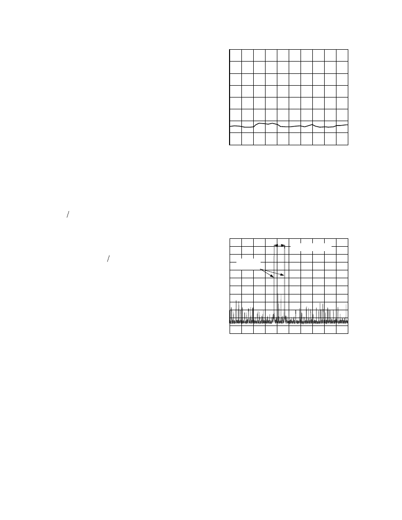
response. To demonstrate the low LO spur level introduced
within the AD9874, Figure 25 plots the demodulated output
power as a function of the input IF frequency for an LO frequency
of 71.1 MHz and a clock frequency of 18 MHz.
90
50
0
–40
–20
–80
–60
100
IF FREQUENCY – MHz
–120
–100
60
70
80
D =
f
CLK
/4 = 4.5MHz
DESIRED
RESPONSES
Figure 25. Response of AD9874 to a –20 dBm
Input IF Input when f
LO
= 71.1 MHz
The two large –10 dBFS spikes near the center of the plot are the
desired responses at
f
LO
±
f
IF2_ADC
where
f
IF2_ADC
=
f
CLK
/8, i.e.,
at 68.85 MHz and 73.35 MHz. LO spurs at
f
LO
±
f
SPUR
would
result in spurious responses at offsets of
±
f
SPUR
around the desired
responses. Close-in spurs of this kind are not visible on the plot,
but small spurious responses at
f
LO
±
f
IF2_ADC
±
f
CLK
, i.e., at
50.85 MHz, 55.35 MHz, 86.85 MHz, and 91.35 MHz, are visible
at the –90 dBFS level. This data indicates that the AD9874 does
an excellent job of preserving the purity of the LO signal.
Figure 25 can also be used to gauge how well the AD9874 rejects
undesired signals. For example, the half-IF response (at 69.975 MHz
and 72.225 MHz) is approximately –100 dBFS, giving a selectivity
of 90 dB for this spurious response. The largest spurious response
at approximately –70 dBFS occurs with input frequencies of
70.35 MHz and 71.85 MHz. These spurs result from third
order nonlinearity in the signal path (i.e.,
abs
[3
f
LO
– 3
f
IF_Input
] =
f
CLK
/8).
相關PDF資料 |
PDF描述 |
|---|---|
| AD9875BSTRL | Broadband Modem Mixed-Signal Front End |
| AD9875 | Broadband Modem Mixed-Signal Front End |
| AD9875-EB | Broadband Modem Mixed-Signal Front End |
| AD9875BST | Broadband Modem Mixed-Signal Front End |
| AD9876 | Broadband Modem Mixed-Signal Front End |
相關代理商/技術參數 |
參數描述 |
|---|---|
| AD9874-EB | 制造商:Analog Devices 功能描述: |
| AD9874-EBZ | 功能描述:BOARD EVAL FOR AD9874 制造商:analog devices inc. 系列:- 零件狀態:有效 類型:數字轉換器 頻率:10MHz ~ 300MHz 配套使用產品/相關產品:AD9874 所含物品:板 標準包裝:1 |
| AD9875 | 制造商:AD 制造商全稱:Analog Devices 功能描述:Broadband Modem Mixed-Signal Front End |
| AD9875BST | 制造商:Analog Devices 功能描述:Modem Chip Single 48-Pin LQFP 制造商:Rochester Electronics LLC 功能描述:10B BROADBAND MODEM MXFE CONVERTER - Tape and Reel |
| AD9875BSTRL | 制造商:Analog Devices 功能描述:Modem Chip Single 48-Pin LQFP T/R |
發布緊急采購,3分鐘左右您將得到回復。