- 您現(xiàn)在的位置:買賣IC網(wǎng) > PDF目錄373970 > AD9876BST (ANALOG DEVICES INC) Broadband Modem Mixed-Signal Front End PDF資料下載
參數(shù)資料
| 型號: | AD9876BST |
| 廠商: | ANALOG DEVICES INC |
| 元件分類: | 通信及網(wǎng)絡(luò) |
| 英文描述: | Broadband Modem Mixed-Signal Front End |
| 中文描述: | SPECIALTY TELECOM CIRCUIT, PQFP48 |
| 封裝: | LQFP-48 |
| 文件頁數(shù): | 17/24頁 |
| 文件大小: | 666K |
| 代理商: | AD9876BST |
REV. A
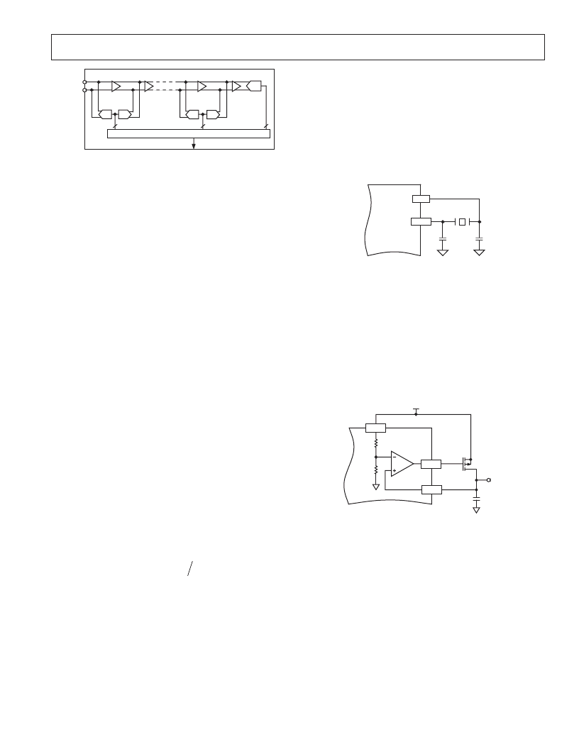
AD9876
–17–
A/D
AINP
AINN
SHA
GAIN
SHA
GAIN
D/A
A/D
D/A
CORRECTION LOGIC
A/D
AD9876
Figure 2. ADC Theory of Operation
The digital data outputs of the ADC are represented in two’s
complement format. They saturate to full scale or zero when the
input signal exceeds the input voltage range.
The twos complement data format is shown below:
011 . . 11: Maximum
000 . . 01: Midscale + 1 LSB
000 . . 00: Midscale
111 . . 11: Midscale – 1 LSB
111 . . 10: Midscale – 2 LSB
100 . . 00: Minimum
The maximum value will be output from the ADC when the
Rx+ input is 1 V or more greater than the Rx– input. The mini-
mum value will be output from the ADC when the Rx– input is
1 V or more greater than the Rx+ input. This results in a full-
scale ADC voltage of 2 Vppd.
The data can be translated to straight binary data format by
simply inverting the most significant bit.
The best ADC performance will be achieved when the ADC
clock source is selected from f
OSCIN
and the OSCIN pin is driven
from a low jitter clock source. The amount of degradation from
jitter on the ADC clock will depend on how quickly the input is
varying at the sampling instance. TPC 36 charts this effect in
the form of
ENOB
vs. input frequency for the two clocking
scenarios.
The maximum sample rate of the ADC in Full-Precision Mode,
that is outputting 12 bits, is 55 MSPS. TPC 33 shows the ADC
performance in ENOB versus f
ADC
. The maximum sample rate
of the ADC in Half-Precision Mode, that is outputting five bits,
is 64 MSPS. The timing of the interface is fully described in the
Receive Port Timing section of this data sheet.
DIGITAL HPF
Following the ADC, there is a bypassable digital HPF. The
response is a single-pole IIR HPF. The transfer function is:
H z
where the sampling period is equal to the ADC clock period.
This results in a 3 dB frequency approximately 1/400th of the
ADC sampling rate. The transfer functions are plotted for
32 MSPS and 50 MSPS in TPC 29 and TPC 32.
The digital HPF introduces a 1 ADC clock cycle latency. If the
HPF function is not desired, the HPF can be bypassed and the
latency will not be incurred.
Z
Z
=
(
) (
)
1 0 99994
– .
1 98466
–
1
1
–
–
CLOCK AND OSCILLATOR CIRCUITRY
The AD9876’s internal oscillator generates all sampling clocks
from a fundamental frequency quartz crystal. Figure 3a shows
how the quartz crystal is connected between OSCIN (Pin 1) and
XTAL (Pin 48) with parallel resonant load capacitors as speci-
fied by the crystal manufacturer. The internal oscillator circuitry
can also be overdriven by a TTL-level clock applied to OSCIN
with XTAL left unconnected.
The PLL has a frequency capture range between 10 MHz
and 64 MHz.
XTAL
C2
AD9876
OSCIN
C1
XTAL
Y1
Figure 3a. Connections for a Fundamental Mode Crystal
VOLTAGE REGULATOR CONTROLLER
The AD9876 contains an on-chip voltage regulator controller
(VRC) for providing a linear 1.3 V supply for low voltage digital
circuitry or other external use. The VRC consists of an op amp
and a resistive voltage divider. As shown in Figure 3b, the resis-
tive divider establishes a voltage of 1.3 V at the inverting input
of the amplifier when DVDD is equal to its nominal voltage of
3.3 V. The feedback loop around the op amp will adjust the gate
voltage such that the voltage at the FB pin, V
FB
, will be equal to
the voltage at the inverting input of the op amp.
DVDD
GATE
FB
V
FB
= 1.3V
V
OUT
SI2301
1.3R
2R
3.3V
S
G
D
C
AD9876
Figure 3b. Connections for 1.3 V Linear Regulator
The maximum current output from the circuit is largely depen-
dent on the MOSFET device. For the SI2301 shown, 250 mA
can be delivered. The regulated output voltage should have bulk
decoupling and high frequency decoupling capacitors to ground
as required by the load. The regulator circuit will be stable for
capacitive loads between 0.1
μ
F and 47
μ
F.
It should be noted that the regulated output voltage, V
FB
, is
proportional to DVDD. Therefore, the percentage variation in
DVDD will also be seen at the regulated output voltage. The
load regulation is roughly equal to the ON resistance of the
MOSFET device chosen. For the SI2301, this is about 60 m
.
相關(guān)PDF資料 |
PDF描述 |
|---|---|
| AD9876BSTRL | Broadband Modem Mixed-Signal Front End |
| AD9877 | Mixed-Signal Front End Set-Top Box, Cable Modem |
| AD9877ABS | Mixed-Signal Front End Set-Top Box, Cable Modem |
| AD9877-EB | Mixed-Signal Front End Set-Top Box, Cable Modem |
| AD9882KST-100 | Dual Interface for Flat Panel Displays |
相關(guān)代理商/技術(shù)參數(shù) |
參數(shù)描述 |
|---|---|
| AD9876BSTRL | 制造商:Rochester Electronics LLC 功能描述:- Tape and Reel |
| AD9876EB | 制造商:Analog Devices 功能描述: |
| AD9876-EB | 制造商:AD 制造商全稱:Analog Devices 功能描述:Broadband Modem Mixed-Signal Front End |
| AD9877 | 制造商:AD 制造商全稱:Analog Devices 功能描述:Mixed-Signal Front End Set-Top Box, Cable Modem |
| AD9877ABS | 制造商:Rochester Electronics LLC 功能描述: 制造商:Analog Devices 功能描述: |
發(fā)布緊急采購,3分鐘左右您將得到回復。