- 您現在的位置:買賣IC網 > PDF目錄373971 > AD9945KCPZRL7 (ANALOG DEVICES INC) Complete 12-Bit 40 MHz CCD Signal Processor PDF資料下載
參數資料
| 型號: | AD9945KCPZRL7 |
| 廠商: | ANALOG DEVICES INC |
| 元件分類: | 消費家電 |
| 英文描述: | Complete 12-Bit 40 MHz CCD Signal Processor |
| 中文描述: | SPECIALTY CONSUMER CIRCUIT, QCC32 |
| 封裝: | 5 X 5 MM, LEAD FREE, MO-220-VHHD-2, LFCSP-32 |
| 文件頁數: | 10/16頁 |
| 文件大小: | 180K |
| 代理商: | AD9945KCPZRL7 |
REV. A
–10–
AD9945
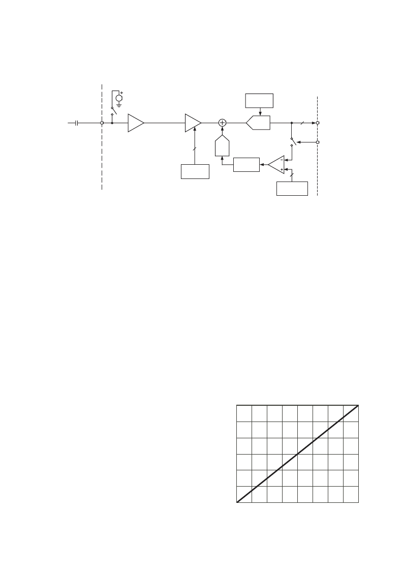
CIRCUIT DESCRIPTION AND OPERATION
The AD9945 signal processing chain is shown in Figure 6. Each
processing step is essential in achieving a high quality image from
the raw CCD pixel data.
DC Restore
To reduce the large dc offset of the CCD output signal, a dc
restore circuit is used with an external 0.1
μ
F series coupling
capacitor. This restores the dc level of the CCD signal to
approximately 1.5 V to be compatible with the 3 V single supply
of the AD9945.
Correlated Double Sampler
The CDS circuit samples each CCD pixel twice to extract the
video information and reject low frequency noise. The timing
shown in Figure 8 illustrates how the two CDS clocks, SHP and
SHD, are used to sample the reference level and data level of
the CCD signal, respectively. The CCD signal is sampled on the
rising edges of SHP and SHD. Placement of these two clock
signals is critical in achieving the best performance from the CCD.
An internal SHP/SHD delay (t
ID
) of 3 ns is caused by internal
propagation delays.
Optical Black Clamp
The optical black clamp loop is used to remove residual offsets
in the signal chain and to track low frequency variations in the
CCD’s black level. During the optical black (shielded) pixel
interval on each line, the ADC output is compared with the
fixed black level reference, selected by the user in the clamp
level register. The resulting error signal is filtered to reduce
noise, and the correction value is applied to the ADC input
through a D/A converter. Normally, the optical black clamp
loop is turned on once per horizontal line, but this loop can be
updated more slowly to suit a particular application. If external
digital clamping is used during the postprocessing, the AD9945
optical black clamping may be disabled using Bit D3 in the
operation register (see the Serial Interface Timing and Internal
Register Description sections).
When the loop is disabled, the clamp level register may still be
used to provide programmable offset adjustment.
Horizontal timing is shown in Figure 9. The CLPOB pulse should
be placed during the CCD’s optical black pixels. It is recom-
mended that the CLPOB pulse be used during valid CCD dark
pixels. The CLPOB pulse should be a minimum of 20 pixels wide
to minimize clamp noise. Shorter pulse widths may be used, but
clamp noise may increase and the loop’s ability to track low fre-
quency variations in the black level will be reduced.
A/D Converter
The ADC uses a 2 V input range. Better noise performance results
from using a larger ADC full-scale range. The ADC uses a
pipelined architecture with a 2 V full-scale input for low noise
performance.
Variable Gain Amplifier
The VGA stage provides a gain range of 6 dB to 40 dB, program-
mable with 10-bit resolution through the serial digital interface.
The minimum gain of 6 dB is needed to match a 1 V input signal
with the ADC full-scale range of 2 V. A plot of the VGA gain curve
is shown in Figure 7.
VGAGain dB
VGACode
(
dB
dB
)
=
×
)
+
0 035
.
5 3
.
VGA GAIN REGISTER CODE
42
0
V
127
255
383
511
639
767
895
1023
36
30
24
18
12
6
Figure 7. VGA Gain Curve
6dB TO 40dB
CCDIN
DIGITAL
FILTERING
CLPOB
DC RESTORE
OPTICAL BLACK
CLAMP
DOUT
12-BIT
ADC
VGA
8-BIT
DAC
CLAMP LEVEL
REGISTER
8
VGA GAIN
REGISTER
10
CDS
INTERNAL
V
REF
2V FULL SCALE
12
0.1 F
Figure 6. CCD Mode Block Diagram
相關PDF資料 |
PDF描述 |
|---|---|
| AD9945 | Complete 12-Bit 40 MHz CCD Signal Processor |
| AD9945KCP | Complete 12-Bit 40 MHz CCD Signal Processor |
| AD9945KCPRL | Complete 12-Bit 40 MHz CCD Signal Processor |
| AD9945KCPRL7 | Complete 12-Bit 40 MHz CCD Signal Processor |
| AD9945KCPZ2 | Complete 12-Bit 40 MHz CCD Signal Processor |
相關代理商/技術參數 |
參數描述 |
|---|---|
| AD9945KCPZRL72 | 制造商:AD 制造商全稱:Analog Devices 功能描述:Complete 12-Bit 40 MHz CCD Signal Processor |
| AD9948 | 制造商:AD 制造商全稱:Analog Devices 功能描述:10-Bit CCD Signal Processor with Precision Timing⑩ Core |
| AD9948AKCPZ | 制造商:Rochester Electronics LLC 功能描述:- Bulk 制造商:Analog Devices 功能描述: |
| AD9948AKCPZRL | 制造商:Analog Devices 功能描述: |
| AD9948KCP | 制造商:Rochester Electronics LLC 功能描述:10 BIT 25 MSPS, 3V ANALOG FRONT END - Bulk 制造商:Analog Devices 功能描述: |
發布緊急采購,3分鐘左右您將得到回復。