- 您現在的位置:買賣IC網 > PDF目錄373975 > ADC912A (Analog Devices, Inc.) CMOS Microprocessor-Compatible 12-Bit A/D Converter PDF資料下載
參數資料
| 型號: | ADC912A |
| 廠商: | Analog Devices, Inc. |
| 英文描述: | CMOS Microprocessor-Compatible 12-Bit A/D Converter |
| 中文描述: | 微處理器的CMOS兼容的12位A / D轉換器 |
| 文件頁數: | 6/16頁 |
| 文件大小: | 237K |
| 代理商: | ADC912A |
REV. B
ADC912A
–6–
PIN FUNCTION DESCRIPTIONS
Pin
Mnemonic
Description
l
2
3
4 . . . 11
13 . . . 16
AIN
VREFIN
AGND
D
11
. . . D
4
D
3/11
. . . D
0/8
Analog Input. 0 V to 10 V.
Voltage Reference Input. Requires external –5 V reference.
Analog Ground.
Three-state data outputs become active when
CS
and
RD
are brought low.
Individual pin function is dependent upon High Byte Enable (HBEN) input.
DATA BUS OUTPUT,
CS
and
RD
= LOW
Pin 4
Pin 5
Pin 6
Pin 7
Pin 8
Pin 9
Pin 10 Pin 11 Pin 13 Pin 14 Pin 15 Pin 16
Mnemonic
*
D
11
D
10
D
9
D
8
D
7
D
6
D
5
D
4
D
3/11
D
2/10
D
1/9
D
0/8
HBEN = LOW
DB
11
DB
10
DB
9
DB
8
DB
7
DB
6
DB
5
DB
4
DB
3
DB
2
DB
1
DB
0
HBEN = HIGH
DB
11
DB
10
DB
9
DB
8
Low
Low
Low
Low
DB
11
DB
10
DB
9
DB
8
*
D
11
. . . D
0/8
are the ADC data output pins.
DB
11
. . . DB
0
are the 12-bit conversion results. DB
11
is the MSB.
Digital Ground.
Clock Input Pin. An external TTL-compatible clock may be applied to this pin. Alternatively a crystal or
ceramic resonator may be connected between CLK IN (Pin 17) and CLK OUT (Pin 18).
Clock Output Pin. An inverted CLK IN signal appears at CLK OUT when an external clock is used. See
CLK IN (Pin 17) description for crystal (resonator).
High Byte Enable Input. Its primary function is to multiplex the 12 bits of conversion data onto the lower
D
7
. . . D
0/8
outputs (4 MSBs or 8 LSBs). See pin description 4 . . . 11 and 13 . . . 16. Also disables
conversion start when HBEN is high.
READ Input. This active LOW signal, in conjunction with
CS
, is used to enable the output data three
state drivers and initiates a conversion if CS and HBEN are low.
Chip Select Input. This active LOW signal, in conjunction with
RD
, is used to enable the output data
three-state drivers and initiates a conversion if
RD
and HBEN are low.
BUSY
output indicates converter status.
BUSY
is LOW during conversion.
Negative Supply, –12 V or –15 V.
Positive Supply, +5 V.
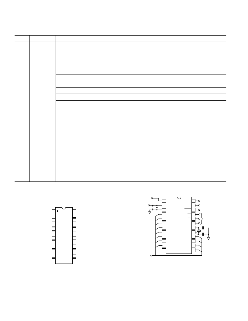
1
2
17
DGND
CLK IN
18
CLK OUT
19
HBEN
20
RD
21
CS
22
23
24
BUSY
V
SS
V
DD
PIN CONFIGURATION
24
23
22
21
20
19
18
17
16
15
14
13
1
2
3
4
5
6
7
8
9
10
11
12
V
DD
V
SS
BUSY
D
0/8
D
1/9
D
2/10
D
3/11
HBEN
CLK OUT
CLK IN
CS
RD
A
IN
V
REFIN
AGND
D
11
D
10
D
9
D
8
D
7
D
6
D
5
D
4
DGND
ADC912A
TOP VIEW
(Not to Scale)
1
2
3
4
5
6
7
8
9
10
11
12
A
IN
V
REFIN
AGND
D
11
D
10
D
9
D
8
D
7
D
6
D
5
D
4
DGND
C1
+
0V TO 10V
ANALOG INPUT
–
5V
REFERENCE
SOURCE
ADC912A
8-BIT OR 16-BIT P DATA BUS
XTAL = 1MHz, C1 = 0.1 F, C3 = 10 F
C3, C4
= 30pF TO 100pF DEPENDING ON XTAL CHOSEN
24
23
22
21
20
19
18
17
16
15
14
13
+5V
–
12V TO
–
15V
STATUS
OUTPUT
P
CONTROL
INPUTS
C3
XTAL
C4
V
DD
V
SS
D
0/8
D
1/9
D
2/10
D
3/11
HBEN
CLK OUT
CLK IN
BUSY
CS
RD
C2
Figure 10. Basic Connection Diagram
相關PDF資料 |
PDF描述 |
|---|---|
| ADC912AFP | CMOS Microprocessor-Compatible 12-Bit A/D Converter |
| ADC912AFS | CMOS Microprocessor-Compatible 12-Bit A/D Converter |
| ADCMP341 | Dual 0.275% Comparators and Reference with Programmable Hysteresis |
| ADCMP341_07 | Dual 0.275% Comparators and Reference with Programmable Hysteresis |
| ADCMP341YRJZ-REEL7 | Dual 0.275% Comparators and Reference with Programmable Hysteresis |
相關代理商/技術參數 |
參數描述 |
|---|---|
| ADC912AFP | 制造商:Analog Devices 功能描述:ADC Single SAR 12-bit Parallel 24-Pin PDIP N 制造商:Analog Devices 功能描述:IC 12BIT ADC CMOS DIP24 912 |
| ADC912AFS | 制造商:Analog Devices 功能描述:ADC Single SAR 12-bit Parallel 24-Pin SOIC W |
| ADC-914MC | 功能描述:模數轉換器 - ADC Analog to Digital Converter RoHS:否 制造商:Texas Instruments 通道數量:2 結構:Sigma-Delta 轉換速率:125 SPs to 8 KSPs 分辨率:24 bit 輸入類型:Differential 信噪比:107 dB 接口類型:SPI 工作電源電壓:1.7 V to 3.6 V, 2.7 V to 5.25 V 最大工作溫度:+ 85 C 安裝風格:SMD/SMT 封裝 / 箱體:VQFN-32 |
| ADC-914MM | 制造商:未知廠家 制造商全稱:未知廠家 功能描述:Analog-to-Digital Converter, 14-Bit |
| ADC9708 | 制造商:未知廠家 制造商全稱:未知廠家 功能描述: |
發布緊急采購,3分鐘左右您將得到回復。