- 您現在的位置:買賣IC網 > PDF目錄373975 > ADC912A (Analog Devices, Inc.) CMOS Microprocessor-Compatible 12-Bit A/D Converter PDF資料下載
參數資料
| 型號: | ADC912A |
| 廠商: | Analog Devices, Inc. |
| 英文描述: | CMOS Microprocessor-Compatible 12-Bit A/D Converter |
| 中文描述: | 微處理器的CMOS兼容的12位A / D轉換器 |
| 文件頁數: | 9/16頁 |
| 文件大小: | 237K |
| 代理商: | ADC912A |
REV. B
ADC912A
–9–
INTERNAL CLOCK OSCILLATOR
Figure 13 shows the ADC912A internal clock circuit. The clock
oscillates at the external crystal or ceramic resonator frequency.
The 1.25 MHz crystal or ceramic resonator connects between
the CLK IN (Pin 17) and the CLK OUT (Pin 18). Capacitance
values (C1, C2) depend on the crystal or ceramic resonator
manufacturer. The crystal vendors should be qualified due to
variations in C1 and C2 values required from vendor to vendor.
Typical values range from 30 pF to 100 pF.
EXTERNAL CLOCK INPUT
A TTL compatible signal connected to CLK IN provides proper
converter clock operation. No connection is necessary to the
CLK OUT pin. The duty cycle of the external clock input can
vary from 45% to 55%. Figure 12 shows the important waveforms.
EXTERNAL REFERENCE
A low output resistance, negative five volt reference is necessary.
The external reference should be able to supply 3 mA of refer-
ence current. A bypass capacitor is necessary on the reference
input lead to minimize system noise as the internal DAC switches.
The reference input to the internal DAC is code dependent requir-
ing anywhere from zero to 3 mA. The reference voltage tolerance
has a direct influence on A/D converter full-scale voltage, and
the maximum input full-scale voltage equals 2
×
–V
REF
. The
ADC912A is designed for ratiometric operation, but operation
using reference voltages between –5.00 V and 0 V will result in
degraded linearity performance. Integral linearity is fully tested and
guaranteed for references of –5 V. Figure 14 provides a good
–5 V reference that does not require precision resistors.
INPUT
V
OUT
TRIM
GND
REF02
+5V TO +15V
10k
100
100
+
V+
V
–
10 F//0.01 F
–
5V
OUTPUT
0.01 F
OP77
2
4
6
5
2
3
–
12V TO
–
15V
TRIM IS OPTIONAL, ONLY NECESSARY
FOR ABSOLUTE ACCURACY CIRCUITS
Figure 14. –5 V Reference
UNIPOLAR ANALOG INPUT OPERATION
Figure 15 shows the ideal input/output characteristic for the 0 V
to 10 V input range of the ADC912A. The designed output
code transitions occur midway between successive integer LSB
values (i.e., 0.5 LSB, 1.5 LSBs, 2.5 LSBs . . . FS – 1.5 LSBs).
The output code is natural binary with 1 LSB = FS/4096 =
(10/4096) V = 2.44 mV. The maximum full-scale input voltage
is (10
×
4095/4096) V = 9.9976 V.
4095
FS
1
1
2
0
4094
FS-1
FS-2
2
0.5
FULL-SCALE
TRANSITION
AT FS
–
1.5 LSB
A
IN
–
ANALOG INPUT IN LSB
D
–
D
Figure 15. Ideal ADC912A Input/Output Transfer
Characteristic
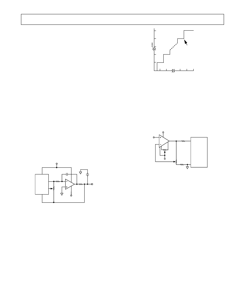
OFFSET AND FULL-SCALE ERROR ADJUSTMENT,
UNIPOLAR OPERATION
For applications where absolute accuracy is important, offset
and full-scale errors can be adjusted to zero. Figure 16 shows
the extra components required for full-scale error adjustment.
Zero offset is achieved by adjusting the null offset of the op amp
driving A
IN
.
10k
20k
200
10
A
IN
AGND
ADC912A
*
ZERO
ADJUST
FULL
SCALE
ADJUST
A1
V
IN
0V TO 10V
3
2
4
1
5
6
7
1
3
+12V
A1: OP27
–
LOWEST NOISE (TRIMMER CONNECTS
BETWEEN PINS 1 & 8, WIPER TO 12V)
OP42
–
BEST BANDWIDTH
*
EXTRA PINS OMITTED FOR CLARITY
–
12V
Figure 16. Unipolar 0 V to 10 V Operation
Adjust the zero scale first by applying 1.22 mV (equivalent to
0.5 LSB input) to V
IN
. Adjust the op amp offset control until
the digital output toggles between 0000 0000 0000 and 0000
0000 0001. The next step is adjustment of full scale. Apply
9.9963 V (equivalent to FS – 1.5 LSB) to V
IN
and adjust R1
until the digital output toggles between 1111 1111 1110 and
1111 1111 1111.
相關PDF資料 |
PDF描述 |
|---|---|
| ADC912AFP | CMOS Microprocessor-Compatible 12-Bit A/D Converter |
| ADC912AFS | CMOS Microprocessor-Compatible 12-Bit A/D Converter |
| ADCMP341 | Dual 0.275% Comparators and Reference with Programmable Hysteresis |
| ADCMP341_07 | Dual 0.275% Comparators and Reference with Programmable Hysteresis |
| ADCMP341YRJZ-REEL7 | Dual 0.275% Comparators and Reference with Programmable Hysteresis |
相關代理商/技術參數 |
參數描述 |
|---|---|
| ADC912AFP | 制造商:Analog Devices 功能描述:ADC Single SAR 12-bit Parallel 24-Pin PDIP N 制造商:Analog Devices 功能描述:IC 12BIT ADC CMOS DIP24 912 |
| ADC912AFS | 制造商:Analog Devices 功能描述:ADC Single SAR 12-bit Parallel 24-Pin SOIC W |
| ADC-914MC | 功能描述:模數轉換器 - ADC Analog to Digital Converter RoHS:否 制造商:Texas Instruments 通道數量:2 結構:Sigma-Delta 轉換速率:125 SPs to 8 KSPs 分辨率:24 bit 輸入類型:Differential 信噪比:107 dB 接口類型:SPI 工作電源電壓:1.7 V to 3.6 V, 2.7 V to 5.25 V 最大工作溫度:+ 85 C 安裝風格:SMD/SMT 封裝 / 箱體:VQFN-32 |
| ADC-914MM | 制造商:未知廠家 制造商全稱:未知廠家 功能描述:Analog-to-Digital Converter, 14-Bit |
| ADC9708 | 制造商:未知廠家 制造商全稱:未知廠家 功能描述: |
發布緊急采購,3分鐘左右您將得到回復。