- 您現(xiàn)在的位置:買賣IC網(wǎng) > PDF目錄373977 > ADCMP572BCP (ANALOG DEVICES INC) Ultrafast 3.3 V Single-Supply Comparators PDF資料下載
參數(shù)資料
| 型號(hào): | ADCMP572BCP |
| 廠商: | ANALOG DEVICES INC |
| 元件分類: | 運(yùn)動(dòng)控制電子 |
| 英文描述: | Ultrafast 3.3 V Single-Supply Comparators |
| 中文描述: | COMPARATOR, 5000 uV OFFSET-MAX, QCC16 |
| 封裝: | MO-220-VEED-2, LFCSP-16 |
| 文件頁數(shù): | 10/16頁 |
| 文件大小: | 412K |
| 代理商: | ADCMP572BCP |
ADCMP572/ADCMP573
Preliminary Technical Data
external 500 resistor, and leaving the LE pin disconnected. In
this case, the resistor value does not depend on the chosen V
CCO
supply voltage, assuming the V
TT
pin is properly connected to
V
CCO
– 2 V.
Rev. PrB | Page 10 of 16
OPTIMIZING HIGH SPEED PERFORMANCE
As with any high speed comparator, proper design and layout
techniques are essential to obtaining the specified performance.
Stray capacitance, inductance, inductive power and ground
impedances, or other layout issues can severely limit performance
and can often cause oscillation. Discontinuities along input and
output transmission lines can also severely limit the specified
pulse-width dispersion performance.
For applications working in a 50 environment, input and
output matching has a significant impact on data dependant (or
deterministic) jitter (DJ) and pulse-width dispersion perform-
ance. The ADCMP572/ADCMP573 comparators provide
internal 50 termination resistors for both V
P
and V
N
inputs,
and the ADCMP572 provides 50 back terminated outputs.
The return side for each input termination is pinned out
separately with the V
TP
and V
TN
pins, respectively. If a 50
termination is desired at one or both of the V
P
/V
N
inputs, then
the V
TP
and V
TN
pins can be connected (or disconnected) to
(from) the desired termination potential as required. The
termination potential should be carefully bypassed using high
quality bypass capacitors as discussed above to prevent undesired
aberrations on the input signal due to parasitic inductance in
the circuit board layout. If a 50 input termination is not
desired, either one or both of the V
TP
/V
TN
termination pins can
be left disconnected. In this case, the pins should be left floating
with no external pull-downs or bypassing capacitors.
It should be understood that when leaving an input termination
disconnected, the internal resistor acts as a small stub on the
input transmission path and can cause problems for very high
speed inputs. Reflections should then be expected from the
comparator inputs because they no longer provide a matched
impedance to the input path leading to the device. It then
becomes important to back-match the drive source impedance
to the input transmission path to minimize multiple reflections.
For applications in which the comparator is very close to the
driving signal source, the source impedance should be mini-
mized. High source impedance in combination with parasitic
input capacitance of the comparator could cause an undesirable
degradation in bandwidth at the input, thus degrading the overall
response. Although the ADCMP572/ ADCMP573 comparators
have been designed to minimize input capacitance, some parasitic
capacitance is inevitable. It is therefore recommended that the
drive source impedance be no more than 50 for best high
speed performance.
COMPARATOR PROPAGATION
DELAY DISPERSION
The ADCMP572/ADCMP573 comparators are designed to
reduce propagation delay dispersion over a wide input overdrive
range of 5 mV to 500 mV. Propagation delay dispersion is a
variation in propagation delay that results from a change in the
degree of overdrive or slew rate (how far or how fast the input
signal exceeds the switching threshold).
Propagation delay dispersion is a specification that becomes
important in high speed time critical applications such as data
communication, automatic test and measurement, instrumenta-
tion, and event-driven applications such as pulse spectroscopy,
nuclear instrumentation, and medical imaging. Dispersion is
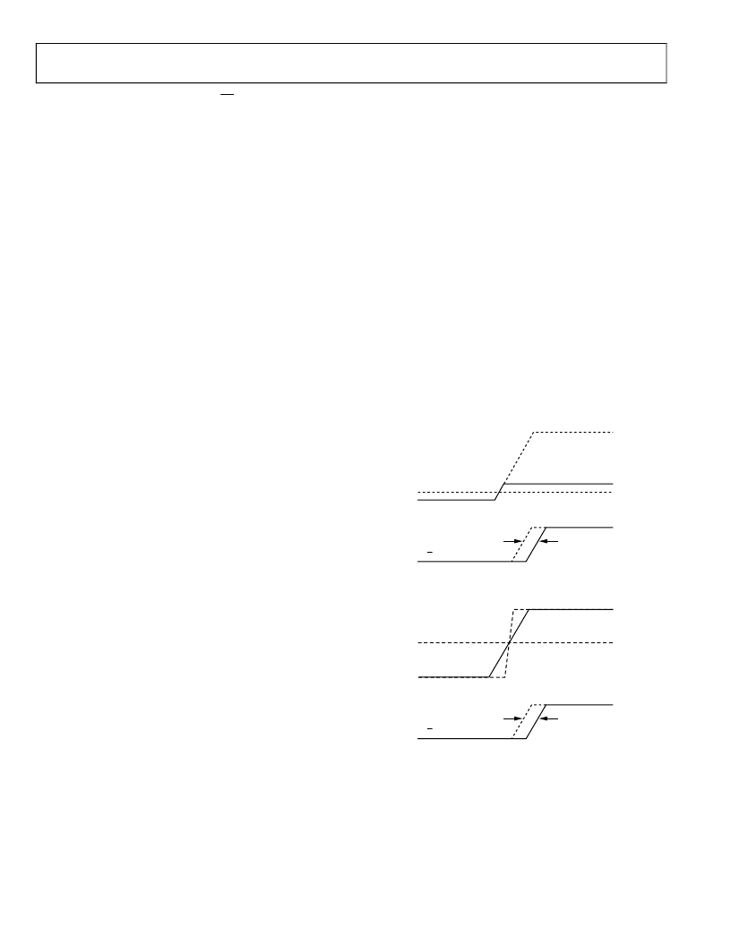
defined as the variation in propagation delay as the input over-
drive conditions are changed (Figure 14 and Figure 15). For the
ADCMP572/ADCMP573, dispersion is typically <15 ps because
the overdrive is varied from 10 mV to 500 mV, and the input
slew rate is varied from 2 V/ns to 10 V/ns. This specification
applies for both positive and negative signals since the
ADCMP572/ADCMP573 has substantially equal delays for
either positive-going or negative-going inputs.
Q/Q OUTPUT
INPUT VOLTAGE
500mV OVERDRIVE
10mV OVERDRIVE
DISPERSION
V
N
± V
OS
0
Figure 14. Propagation Delay—Overdrive Dispersion
Q/Q OUTPUT
INPUT VOLTAGE
10V/ns
1V/ns
DISPERSION
V
N
± V
OS
0
Figure 15. Propagation Delay—Slew Rate Dispersion
相關(guān)PDF資料 |
PDF描述 |
|---|---|
| ADCMP573 | Ultrafast 3.3 V Single-Supply Comparators |
| ADCMP573BCP | Ultrafast 3.3 V Single-Supply Comparators |
| ADCMP580 | Ultrafast SiGe Voltage Comparators |
| ADCMP580_05 | Ultrafast SiGe Voltage Comparators |
| ADCMP580BCP-R2 | Ultrafast SiGe Voltage Comparators |
相關(guān)代理商/技術(shù)參數(shù) |
參數(shù)描述 |
|---|---|
| ADCMP572BCP-R2 | 制造商:Analog Devices 功能描述:Comparator Single 5.4V 16-Pin LFCSP EP T/R 制造商:Rochester Electronics LLC 功能描述:SINGLE SUPPLY, CML ON XFCB3.0- - Bulk |
| ADCMP572BCP-RL7 | 制造商:Analog Devices 功能描述:Comparator Single 5.4V 16-Pin LFCSP EP T/R |
| ADCMP572BCP-WP | 制造商:Analog Devices 功能描述:Comparator Single 5.4V 16-Pin LFCSP EP |
| ADCMP572BCPZ-R2 | 功能描述:IC COMPARATOR CML 3.3-5V 16LFCSP RoHS:是 類別:集成電路 (IC) >> 線性 - 比較器 系列:- 標(biāo)準(zhǔn)包裝:1 系列:- 類型:通用 元件數(shù):1 輸出類型:CMOS,開路集電極,TTL 電壓 - 電源,單路/雙路(±):2.7 V ~ 5.5 V 電壓 - 輸入偏移(最小值):7mV @ 5V 電流 - 輸入偏壓(最小值):0.25µA @ 5V 電流 - 輸出(標(biāo)準(zhǔn)):84mA @ 5V 電流 - 靜態(tài)(最大值):120µA CMRR, PSRR(標(biāo)準(zhǔn)):- 傳輸延遲(最大):600ns 磁滯:- 工作溫度:-40°C ~ 85°C 封裝/外殼:SC-74A,SOT-753 安裝類型:表面貼裝 包裝:剪切帶 (CT) 產(chǎn)品目錄頁面:1268 (CN2011-ZH PDF) 其它名稱:*LMV331M5*LMV331M5/NOPBLMV331M5CT |
| ADCMP572BCPZ-RL7 | 功能描述:IC COMPARATOR CML 3.3-5V 16LFCSP RoHS:是 類別:集成電路 (IC) >> 線性 - 比較器 系列:- 產(chǎn)品培訓(xùn)模塊:Lead (SnPb) Finish for COTS Obsolescence Mitigation Program 標(biāo)準(zhǔn)包裝:2,500 系列:- 類型:通用 元件數(shù):1 輸出類型:CMOS,推挽式,滿擺幅,TTL 電壓 - 電源,單路/雙路(±):2.5 V ~ 5.5 V,±1.25 V ~ 2.75 V 電壓 - 輸入偏移(最小值):5mV @ 5.5V 電流 - 輸入偏壓(最小值):1pA @ 5.5V 電流 - 輸出(標(biāo)準(zhǔn)):- 電流 - 靜態(tài)(最大值):24µA CMRR, PSRR(標(biāo)準(zhǔn)):80dB CMRR,80dB PSRR 傳輸延遲(最大):450ns 磁滯:±3mV 工作溫度:-40°C ~ 85°C 封裝/外殼:6-WFBGA,CSPBGA 安裝類型:表面貼裝 包裝:管件 其它名稱:Q3554586 |
發(fā)布緊急采購,3分鐘左右您將得到回復(fù)。