- 您現在的位置:買賣IC網 > PDF目錄373980 > ADE7754ARRL (ANALOG DEVICES INC) ADE7754 PDF資料下載
參數資料
| 型號: | ADE7754ARRL |
| 廠商: | ANALOG DEVICES INC |
| 元件分類: | 模擬信號調理 |
| 英文描述: | ADE7754 |
| 中文描述: | SPECIALTY ANALOG CIRCUIT, PDSO24 |
| 封裝: | MS-013AD, SOIC-24 |
| 文件頁數: | 3/44頁 |
| 文件大小: | 630K |
| 代理商: | ADE7754ARRL |
第1頁第2頁當前第3頁第4頁第5頁第6頁第7頁第8頁第9頁第10頁第11頁第12頁第13頁第14頁第15頁第16頁第17頁第18頁第19頁第20頁第21頁第22頁第23頁第24頁第25頁第26頁第27頁第28頁第29頁第30頁第31頁第32頁第33頁第34頁第35頁第36頁第37頁第38頁第39頁第40頁第41頁第42頁第43頁第44頁
REV. PrG 01/03
PRELIMINARY TECHNICAL DATA
–3–
ADE7754
ADE7754 TIMING CHARACTERISTICS
1,2
Parameter
Units
Test Conditions/Comments
Write timing
t
1
t
2
t
3
t
4
t
5
t
6
t
7
t
8
Read timing
t
95
50
50
50
10
5
400
50
100
ns (min)
ns (min)
ns (min)
ns (min)
ns (min)
ns (min)
ns (min)
ns (min)
CS
falling edge to first SCLK falling edge
SCLK logic high pulse width
SCLK logic low pulse width
Valid Data Set up time before falling edge of SCLK
Data Hold time after SCLK falling edge
Minimum time between the end of data byte transfers.
Minimum time between byte transfers during a serial write.
CS
Hold time after SCLK falling edge.
4
μ
s (min)
Minimum time between read command (i.e. a write to Communication
Register) and data read.
Minimum time between data byte transfers during a multibyte read.
Data access time after SCLK rising edge following a write to the
Communications Register
Bus relinquish time after falling edge of SCLK.
t
t
10
50
30
ns (min)
ns (min)
t
124
100
10
100
10
ns (max)
ns (min)
ns (max)
ns (min)
t
134
Bus relinquish time after rising edge of
CS
.
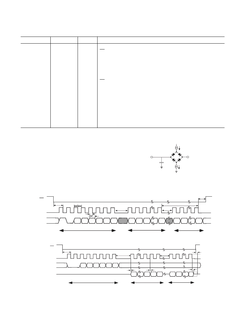
Serial Read Timing
Serial Write Timing
CS
SCLK
DIN
A4 A3 A2
A1 A0
DB7
Most Significant Byte
t
1
t
2
t
3
t
4
t
5
t
8
1
DB0
DB7
DB0
t
6
Least Significant Byte
t
7
t
7
0
Command Byte
A5
CS
SCLK
DIN
A4 A3 A2
A1 A0
t
1
t
11
t
12
t
9
DB7
DOUT
t
13
DB0
DB0
DB7
t
10
t
14
Most Significant
Byte
Least Significant
Byte
0
0
Command
Byte
A5
(AV
DD
= DV
DD
= 5V ± 5%, AGND = DGND = 0V, On-Chip Reference,
CLKIN = 10MHz XTAL, TMIN to TMAX = -40°C to +85°C)
Figure 1 - Load Circuit for Timing Specifications
200 μA
1.6 mA
I
OH
I
OL
C
L
50pF
TO
OUTPUT
PIN
+2.1V
NOTES
1
Sample tested during initial release and after any redesign or process change that may
affect this parameter. All input signals are specified with tr = tf = 5ns (10% to 90%)
and timed from a voltage level of 1.6V.
2
See timing diagram below and Serial Interface section of this data sheet.
3
Measured with the load circuit in Figure 1 and defined as the time required for the
output to cross 0.8V or 2.4V.
4
Derived from the measured time taken by the data outputs to change 0.5V when
loaded with the circuit in Figure 1. The measured number is then extrapolated back
to remove the effects of charging or discharging the 50pF capacitor. This means that
the time quoted in the timing characteristics is the true bus relinquish time of the
part and is independent of the bus loading.
5
Minimum time between read command and data read for all registers
except WAVFORM register. For WAVFORM register t
9
=500ns min
相關PDF資料 |
PDF描述 |
|---|---|
| ADE7755AN-REF | Energy Metering IC with Pulse Output |
| ADE7755ARSRL | Energy Metering IC with Pulse Output |
| ADE7755 | Energy Metering IC with Pulse Output |
| ADE7755ARS | Energy Metering IC with Pulse Output |
| ADE7756EB | Evaluation Board Documentation AD7756 Energy metering IC |
相關代理商/技術參數 |
參數描述 |
|---|---|
| ADE7754ARZ | 功能描述:IC ENERGY METERING 3PHASE 24SOIC RoHS:是 類別:集成電路 (IC) >> PMIC - 能量測量 系列:- 產品培訓模塊:Lead (SnPb) Finish for COTS Obsolescence Mitigation Program 標準包裝:2,500 系列:* |
| ADE7754ARZRL | 功能描述:IC ENERGY METERING 3PHASE 24SOIC RoHS:是 類別:集成電路 (IC) >> PMIC - 能量測量 系列:- 產品培訓模塊:Lead (SnPb) Finish for COTS Obsolescence Mitigation Program 標準包裝:2,500 系列:* |
| ADE7755 | 制造商:AD 制造商全稱:Analog Devices 功能描述:Energy Metering IC with Pulse Output |
| ADE7755AARSRL | 制造商:Analog Devices 功能描述:ENERGY METERING IC WITH P - Tape and Reel |
| ADE7755AN | 制造商:Rochester Electronics LLC 功能描述: 制造商:Analog Devices 功能描述: |
發布緊急采購,3分鐘左右您將得到回復。