- 您現在的位置:買賣IC網 > PDF目錄373983 > ADF4360-4BCP (ANALOG DEVICES INC) Integrated Synthesizer and VCO PDF資料下載
參數資料
| 型號: | ADF4360-4BCP |
| 廠商: | ANALOG DEVICES INC |
| 元件分類: | 無繩電話/電話 |
| 英文描述: | Integrated Synthesizer and VCO |
| 中文描述: | TELECOM, CELLULAR, BASEBAND CIRCUIT, QCC24 |
| 封裝: | 4 X 4 MM, MO-220-VGGD-2, LFCSP-24 |
| 文件頁數: | 8/20頁 |
| 文件大小: | 336K |
| 代理商: | ADF4360-4BCP |
PRELIMINARY TECHNICAL DATA
REV. PrA 07/03
–8–
0
P
ADF4360-2
R COUNTER
The 14-bit R counter allows the input reference frequency
to be divided down to produce the reference clock to the
phase frequency detector (PFD). Division ratios from 1 to
16,383 are allowed.
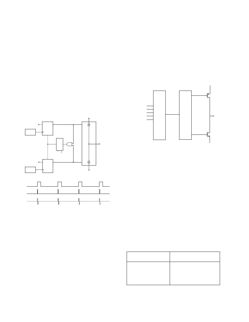
PHASE FREQUENCY DETECTOR (PFD) AND
CHARGE PUMP
The PFD takes inputs from the R counter and N counter
(N=BP+A) and produces an output proportional to the
phase and frequency difference between them. Figure 4 is a
simplified schematic. The PFD includes a programmable
delay element which controls the width of the anti-backlash
pulse. This pulse ensures that there is no deadzone in the
PFD transfer function and minimizes phase noise and
reference spurs. Two bits in the R Counter Latch, ABP2
and ABP1 control the width of the pulse. See Page 14.
Figure 4. PFD Simplified Schematic and Timing (In Lock)
Figure 5. MUXOUT Circuit
INPUT SHIFT REGISTER
The ADF4360 family’s digital section includes a 24-bit
input shift register, a 14-bit R counter and a 18-bit N
counter, comprising a 5-bit A counter and a 13-bit B
counter. Data is clocked into the 24-bit shift register on
each rising edge of CLK. The data is clocked in MSB
first. Data is transferred from the shift register to one of
four latches on the rising edge of LE. The destination
latch is determined by the state of the two control bits
(C2, C1) in the shift register. These are the two lsb's
DB1, DB0 as shown in the timing diagram of Figure 1.
The truth table for these bits is shown in Table 1. Table 2
shows a summary of how the latches are programmed.
Please note that the Test Modes Latch is used for Factory
Testing snd should not be programmed by the user.
Control Bits
C2
C1
Data Latch
0
0
1
1
0
1
0
1
Control Latch
R Counter
N Counter (A & B)
Test Modes Latch
HI
HI
D1
D2
Q1
Q2
CLR1
CLR2
CP
P
D
U1
U2
U3
UP
DOWN
CHARGE
PUMP
ABP2
ABP1
CPGND
V
P
R DIVIDER
N DIVIDER
R DIVIDER
N DIVIDER
CP OUTPUT
Analog Lock Detect
MUXOUT
CONTROL
Digital Lock Detect
R Counter Output
N Counter Output
SDOUT
MUX
DV
DD
DGND
Table I. C2, C1 Truth Table
MUXOUT AND LOCK DETECT
The output multiplexer on the ADF4360 family allows
the user to access various internal points on the chip. The
state of MUXOUT is controlled by M3, M2 and M1 in
the Function Latch. The full truth table is shown on page
13. Figure 5 shows the MUXOUT section in block
diagram form.
Lock Detect
MUXOUT can be programmed for two types of lock
detect: digital lock detect and analog lock detect.
Digital lock detect is active high. When LDP in the R
Counter latch is set to 0, digital lock detect is set high
when the phase error on three consecutive Phase Detector
cycles is less than 15ns.
With LDP set to "1", five consecutive cycles of less than
15ns phase error are required to set the lock detect. It will
stay set high until a phase error of greater than 25ns is
detected on any subsequent PD cycle.
The N-channel open-drain analog lock detect should be
operated with an external pull-up resistor of 10k
nominal. When lock has been detected this output will be
high with narrow low-going pulses.
相關PDF資料 |
PDF描述 |
|---|---|
| ADF4360-1BCP | Integrated Synthesizer and VCO |
| ADF4360-2 | Integrated Synthesizer and VCO |
| ADF4360-2BCP | Integrated Synthesizer and VCO |
| ADF4360-6BCP | Integrated Synthesizer and VCO |
| ADF4360-7BCP | Integrated Synthesizer and VCO |
相關代理商/技術參數 |
參數描述 |
|---|---|
| ADF4360-4BCPRL | 制造商:Analog Devices 功能描述:PLL Frequency Synthesizer Single 24-Pin LFCSP EP T/R |
| ADF4360-4BCPRL7 | 制造商:Analog Devices 功能描述:PLL Frequency Synthesizer Single 24-Pin LFCSP EP T/R |
| ADF4360-4BCPZ | 功能描述:IC INT SYNTH/VCO SEALED 24-LFCSP RoHS:是 類別:集成電路 (IC) >> 時鐘/計時 - 時鐘發生器,PLL,頻率合成器 系列:- 標準包裝:2,000 系列:- 類型:PLL 頻率合成器 PLL:是 輸入:晶體 輸出:時鐘 電路數:1 比率 - 輸入:輸出:1:1 差分 - 輸入:輸出:無/無 頻率 - 最大:1GHz 除法器/乘法器:是/無 電源電壓:4.5 V ~ 5.5 V 工作溫度:-20°C ~ 85°C 安裝類型:表面貼裝 封裝/外殼:16-LSSOP(0.175",4.40mm 寬) 供應商設備封裝:16-SSOP 包裝:帶卷 (TR) 其它名稱:NJW1504V-TE1-NDNJW1504V-TE1TR |
| ADF4360-4BCPZ | 制造商:Analog Devices 功能描述:IC FREQ SYNTHESIZER & VCO 1.45GHZ LFCSP 制造商:Analog Devices 功能描述:IC, FREQ SYNTHESIZER & VCO 1.45GHZ LFCSP |
| ADF4360-4BCPZKL1 | 制造商:Analog Devices 功能描述: |
發布緊急采購,3分鐘左右您將得到回復。