- 您現(xiàn)在的位置:買賣IC網(wǎng) > PDF目錄373989 > ADG633 (Analog Devices, Inc.) Tantalum Molded Capacitor; Capacitance: 22uF; Voltage: 6.3V; Case Size: 1.6x3.2 mm; Packaging: Tape & Reel PDF資料下載
參數(shù)資料
| 型號(hào): | ADG633 |
| 廠商: | Analog Devices, Inc. |
| 英文描述: | Tantalum Molded Capacitor; Capacitance: 22uF; Voltage: 6.3V; Case Size: 1.6x3.2 mm; Packaging: Tape & Reel |
| 中文描述: | 的CMOS第V / 5伏/ 3伏三SPDT開關(guān) |
| 文件頁數(shù): | 5/12頁 |
| 文件大小: | 546K |
| 代理商: | ADG633 |
ADG633
–5–
ABSOLUTE MAXIMUM RATINGS
1
(T
A
= 25°C, unless otherwise noted.)
V
DD
to V
SS
. . . . . . . . . . . . . . . . . . . . . . . . . . . . . . . . . . . . . . 13 V
V
DD
to GND . . . . . . . . . . . . . . . . . . . . . . . . . . –0.3 V to +13 V
V
SS
to GND . . . . . . . . . . . . . . . . . . . . . . . . . . . +0.3 V to –6.5 V
Analog Inputs
2
. . . . . . . . . . . . . . . . . .V
SS
– 0.3 V to V
DD
+ 0.3 V
Digital Inputs
2
. . . . . . . . . . . . . . . .GND – 0.3 V to V
DD
+ 0.3 V
Peak Current, S or D . . . . . . . . . . . . . . . . . . . . . . . . . . . 40 mA
(Pulsed at 1 ms, 10% duty cycle max)
Continuous Current, S or D . . . . . . . . . . . . . . . . . . . . . 20 mA
Operating Temperature Range
Automotive (Y Version) . . . . . . . . . . . . . . . –40°C to +125°C
Industrial (B Version) . . . . . . . . . . . . . . . . . . –40°C to +85°C
Storage Temperature Range . . . . . . . . . . . . . . –65°C to +150°C
or 10 mA, whichever occurs first
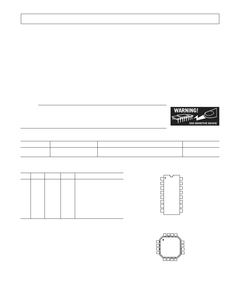
PIN CONFIGURATIONS
TSSOP
TOP VIEW
(Not to Scale)
16
15
14
13
12
11
10
9
1
2
3
4
5
6
7
S2B
S2A
S3B
D3
S3A
V
SS
EN
GND
V
DD
D2
D1
S1B
S1A
A0
A1
A2
8
LFCSP
ADG633
TOP VIEW
(Not to Scale)
11
10
9
8
7
6
5
4
3
2
1
12
13
14
15
16
S3B
D3
V
A
S1A
A0
D1
S1B
EN
S3A
D
V
S
S
A
G
ORDERING GUIDE
Package Description
Thin Shrink Small Outline Package (TSSOP)
Chip Scale Package (LFCSP)
Model
ADG633YRU
ADG633YCP
Temperature Range
–40°C to +125°C
–40°C to +85°C
Package Option
RU-16
CP-16
Junction Temperature . . . . . . . . . . . . . . . . . . . . . . . . . . 150°C
JA
Thermal Impedance, 16-Lead TSSOP . . . . . . . .150.4°C/W
JA
Thermal Impedance (4-Layer Board),
16-Lead LFCSP . . . . . . . . . . . . . . . . . . . . . . . . . . . 70°C/W
Lead Temperature, Soldering
Vapor Phase (60 sec) . . . . . . . . . . . . . . . . . . . . . . . . . 215°C
Infrared (15 sec) . . . . . . . . . . . . . . . . . . . . . . . . . . . . 220°C
ESD . . . . . . . . . . . . . . . . . . . . . . . . . . . . . . . . . . . . . . . . . . 4 kV
NOTES
1
Stresses above those listed under Absolute Maximum Ratings may cause permanent
damage to the device. This is a stress rating only; functional operation of the device
at these or any other conditions above those listed in the operational sections of this
specification is not implied. Exposure to absolute maximum rating conditions for
extended periods may affect device reliability. Only one absolute maximum rating
may be applied at any one time.
2
Overvoltages at A
X
,
EN
, S, or D will be clamped by internal diodes. Current should
be limited to the maximum ratings given.
Table I. ADG633 Truth Table
A0
EN
X
1
0
0
1
0
0
0
1
0
0
0
1
0
0
0
1
0
A2
X
0
0
0
0
1
1
1
1
A1
X
0
0
1
1
0
0
1
1
Switch Condition
NONE
D1–S1A, D2–S2A, D3–S3A
D1–S1B, D2–S2A, D3–S3A
D1–S1A, D2–S2B, D3–S3A
D1–S1B, D2–S2B, D3–S3A
D1–S1A, D2–S2A, D3–S3B
D1–S1B, D2–S2A, D3–S3B
D1–S1A, D2–S2B, D3–S3B
D1–S1B, D2–S2B, D3–S3B
X = Don’t Care
CAUTION
ESD (electrostatic discharge) sensitive device. Electrostatic charges as high as 4000 V readily ac cu mu ate
on the human body and test equipment and can discharge without detection. Although the ADG633
features proprietary ESD pro ec ion circuitry, permanent damage may occur on devices subjected to high
energy electrostatic discharges. Therefore, proper ESD pre cau ions are rec om mend ed to avoid per or mance
deg a da ion or loss of functionality.
REV. 0
相關(guān)PDF資料 |
PDF描述 |
|---|---|
| ADG633YCP | CMOS +V/+5 V/+3 V Triple SPDT Switch |
| ADG636 | 1 pC Charge Injection, 100 pA Leakage CMOS 5 V/+5 V/+3 V Dual SPDT Switch |
| ADG636YRU | 1 pC Charge Injection, 100 pA Leakage CMOS 5 V/+5 V/+3 V Dual SPDT Switch |
| ADG658YRU | +3 V/+5 V/【5 V CMOS 4-/8-Channel Analog Multiplexers |
| ADG658 | +3 V/+5 V/【5 V CMOS 4-/8-Channel Analog Multiplexers |
相關(guān)代理商/技術(shù)參數(shù) |
參數(shù)描述 |
|---|---|
| ADG633_09 | 制造商:AD 制造商全稱:Analog Devices 功能描述:CMOS, ?±5 V/5 V/3 V, Triple SPDT Switch |
| ADG633YCP | 制造商:Analog Devices 功能描述:Analog Switch Triple SPDT 16-Pin LFCSP EP 制造商:Rochester Electronics LLC 功能描述:2:1 MUX, +/-5V SUPPLY RATE TO +125: I.C. - Bulk |
| ADG633YCP-REEL7 | 制造商:Analog Devices 功能描述:Analog Switch Triple SPDT 16-Pin LFCSP EP T/R 制造商:Rochester Electronics LLC 功能描述:2:1 MUX, +/-5V SUPPLY RATE TO +125: I.C. - Tape and Reel |
| ADG633YCPZ | 功能描述:IC SWITCH TRIPLE SPDT 16LFCSP RoHS:是 類別:集成電路 (IC) >> 接口 - 模擬開關(guān),多路復(fù)用器,多路分解器 系列:- 應(yīng)用說明:Ultrasound Imaging Systems Application Note 產(chǎn)品培訓(xùn)模塊:Lead (SnPb) Finish for COTS Obsolescence Mitigation Program 標(biāo)準(zhǔn)包裝:250 系列:- 功能:開關(guān) 電路:單刀單擲 導(dǎo)通狀態(tài)電阻:48 歐姆 電壓電源:單電源 電壓 - 電源,單路/雙路(±):2.7 V ~ 5.5 V 電流 - 電源:5µA 工作溫度:0°C ~ 70°C 安裝類型:表面貼裝 封裝/外殼:48-LQFP 供應(yīng)商設(shè)備封裝:48-LQFP(7x7) 包裝:托盤 |
| ADG633YCPZ1 | 制造商:AD 制造商全稱:Analog Devices 功能描述:CMOS, ?±5 V/5 V/3 V, Triple SPDT Switch |
發(fā)布緊急采購,3分鐘左右您將得到回復(fù)。