- 您現(xiàn)在的位置:買賣IC網(wǎng) > PDF目錄373994 > ADL5390-EVAL (Analog Devices, Inc.) RF/IF Vector Multiplier PDF資料下載
參數(shù)資料
| 型號: | ADL5390-EVAL |
| 廠商: | Analog Devices, Inc. |
| 英文描述: | RF/IF Vector Multiplier |
| 中文描述: | 射頻中頻向量乘法器/ |
| 文件頁數(shù): | 12/24頁 |
| 文件大小: | 716K |
| 代理商: | ADL5390-EVAL |
ADL5390
APPLICATIONS
USING THE ADL5390
The ADL5390 is designed to operate in a 50 impedance system.
Figure 29 illustrates an example where the RF/IF inputs are
driven in a single-ended fashion, while the differential RF out-
put is converted to a single-ended output with a RF balun. The
baseband gain controls for the I and Q channels are typically
driven from differential DAC outputs. The power supplies,
VPRF and VPS2, should be bypassed appropriately with 0.1 μF
and 100 pF capacitors. Low inductance grounding of the CMOP
and CMRF common pins is essential to prevent unintentional
peaking of the gain. The exposed paddle on the underside of the
package should be soldered to a low thermal and electrical
impedance ground plane.
Rev. 0 | Page 12 of 24
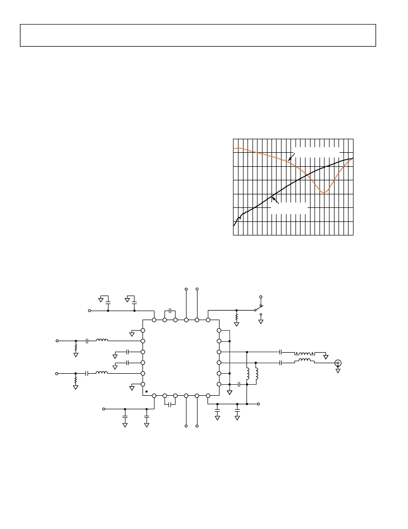
RF INPUT AND MATCHING
The RF/IF inputs present 250
resistive terminations to
ground. In general, the input signals should be ac-coupled
through dc-blocking capacitors. The inputs may be driven dif-
ferentially or single-ended, in which case the unused inputs are
connected to common via the dc-blocking capacitors. The
ADL5390’s performance is not degraded by driving these inputs
single-ended. The input impedance can be reduced by placing
external shunt termination resistors to common on the source
side of the dc-blocking capacitors so that the quiescent dc-bias
level of the ADL5390 inputs is not affected, as shown in Figure
29. Capacitive reactance at the RF inputs can be compensated
for with series inductance. In fact, the customer evaluation
board has high impedance line traces between the shunt termi-
nation pads and the device input pins, which provides series in-
ductance and improves the return loss at 1.9 GHz to better than
15 dB with the shunt termination removed, as shown in Figure
28.
S11 MATCH WITHOUT
66.5
TERMINATION
S11 MATCH WITH
TERMINATION
0
–5
–10
–15
–20
–25
–30
–35
d
2
3
5
8
1
1
1
2
2
1
2
4
4
6
7
9
1
1
1
1
1
1
1
2
2
2
FREQUENCY (MHz)
0
Figure 28. ADL5390 Customer Evaluation Board RF Input Return Loss.
0
C12
(SEE TEXT)
C11
(SEE TEXT)
C8
100pF
VP
C7
0.1
μ
F
VP
C4
0.1
μ
F
B
A
SW1
R8
10k
VP
IBBM
IBBP
QBBP QBBM
L2
0
C5
10nF
RFIN_Q
R22
66.5
L1
0
C2
10nF
RFIN_I
R2
66.5
C1
10nF
C6
10nF
L4
120nH
L3
120nH
C14
0.1
μ
F
C10
100pF
C9
0.1
μ
F
VP
C17
10nF
C18
10nF
RFOP
1
5
3
4
T1
ETC1-1-13
(M/A-COM)
I
I
VPS2
DSOP
CMOP
Q
Q
VPRF
CMRF
INMI
IPMQ
CMOP
RFOM
RFOP
Q
Q
CMOP
CMOP
CMRF
VPRF
I
I
ADL5390
INPI
INPQ
C3
100pF
Figure 29. Basic Connections
相關(guān)PDF資料 |
PDF描述 |
|---|---|
| ADL5390ACPZ-REEL71 | RF/IF Vector Multiplier |
| ADL5390ACPZ-WP1 | RF/IF Vector Multiplier |
| ADL5390 | RF/IF Vector Multiplier |
| ADL5391 | DC to 2.0 GHz Multiplier |
| ADL5391ACPZ-R2 | DC to 2.0 GHz Multiplier |
相關(guān)代理商/技術(shù)參數(shù) |
參數(shù)描述 |
|---|---|
| ADL5390-EVALZ | 制造商:Analog Devices 功能描述:Evaluation Board For ADL5390 制造商:Analog Devices 功能描述:EVALUATION BOARDS - Bulk |
| ADL5391 | 制造商:AD 制造商全稱:Analog Devices 功能描述:DC to 2.0 GHz Multiplier |
| ADL5391ACPZ | 制造商:Analog Devices 功能描述:IC, MULTIPLIER, 2.0GHZ, 16LFCSP 制造商:Analog Devices 功能描述:IC, MULTIPLIER, 2.0GHZ, 16LFCSP; IC Function:Analogue Multiplier; Brief Features:3 dB bandwidth of 2 GHz; Supply Voltage Min:4.5V; Supply Voltage Max:5.5V; Operating Temperature Min:-40C; Operating Temperature Max:85C; Digital IC ;RoHS Compliant: Yes |
| ADL5391ACPZ-R2 | 制造商:Analog Devices 功能描述:DC TO 2.0 GHZ MULTIPLIER - Tape and Reel |
| ADL5391ACPZ-R7 | 功能描述:IC MULTIPLIER 2.0GHZ 16LFCSP RoHS:是 類別:RF/IF 和 RFID >> RF 其它 IC 和模塊 系列:- 標(biāo)準(zhǔn)包裝:100 系列:* |
發(fā)布緊急采購,3分鐘左右您將得到回復(fù)。