- 您現(xiàn)在的位置:買賣IC網(wǎng) > PDF目錄374016 > ADMC330BST (ANALOG DEVICES INC) Single Chip DSP Motor Controller PDF資料下載
參數(shù)資料
| 型號: | ADMC330BST |
| 廠商: | ANALOG DEVICES INC |
| 元件分類: | 數(shù)字信號處理 |
| 英文描述: | Single Chip DSP Motor Controller |
| 中文描述: | 0-BIT, 20 MHz, OTHER DSP, PQFP80 |
| 封裝: | PLASTIC, TQFP-80 |
| 文件頁數(shù): | 10/20頁 |
| 文件大小: | 163K |
| 代理商: | ADMC330BST |
ADMC330
–10–
REV. 0
V1
PWMSYNC
VVIL
COMPARATOR
OUTPUT
t
V
C
V
CMAX
T
CRST
t
VIL
T
PWM
– T
CRST
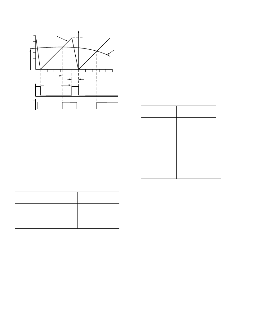
Figure 6. Analog Input Block Operation
ADC Resolution
Because the operation of the ADC is intrinsically linked to the
PMW block, the effective resolution of the ADC is a function of
the PMW switching frequency. T he effective ADC resolution is
determined by the rate at which the counter timer is clocked.
For a CLK IN period of t
CK
and a PWM period of T
PWM
, the
maximum count of the ADC is given by
Max Count
=
T
PWM
t
CK
For an assumed CLK IN frequency of 10 MHz, the effective
resolution of the ADC block is tabulated for various PWM
switching frequencies in T able II.
T able II. ADC Resolution E xamples
PWM Frequency
(kHz)
E ffective Resolution
(Bits)
Max Count
2.5
4
8
18
25
3980
2480
1230
535
380
≈
12
>11
>10
>9
>8
E xternal T iming Capacitor
In order to maximize the useful input voltage range and effective
resolution of the ADC, it is necessary to carefully select the
value of the external timing capacitor. For a given capacitance
value, C
NOM
, the peak ramp voltage is given by:
V
C
max
=
I
CONST
T
PWM
±
T
CRST
(
C
NOM
)
where
I
CONST
is the nominal current source value of 10.5
μ
A and
T
CRST
is the PWMSYNC pulsewidth. In selecting the capacitor
value, however, it is necessary to take into account the tolerance
of the capacitor and the variation of the current source value.
T o ensure that the full input range of the ADC is utilized, it is
necessary to select the capacitor so that at the maximum capaci-
tance value and the minimum current source output, the ramp
voltage will charge to at least 3.5 V.
As a result, assuming
±
10% variations in both the capacitance
and current source, the nominal capacitance value required at a
given PWM period is:
C
NOM
=
(0.9
×
I
CONST
)(
T
PWM
±
T
CRST
)
(1.1)(3.5)
T he largest standard value capacitor that is less than this calcu-
lated value is chosen. T able III shows the appropriate standard
capacitor value to use for various PWM switching frequencies
assuming
±
10% variations in both the current source and ca-
pacitor tolerances. If required, more precise control of the ramp
voltage is possible by using higher precision capacitor compo-
nents, an external current source and/or series or parallel timing
capacitor combinations.
T able III. T iming Capacitor Selection
PWM Frequency
(kHz)
T iming Capacitor
(pF)
2.5–3.0
3.0–3.6
3.6–4.3
4.3–5.2
5.2–6.2
6.2–7.3
7.3–9.0
9.0–10.9
10.9–13.2
13.2–15.8
15.8–19.6
19.6–23.4
23.4–28.2
820
680
560
470
390
330
270
220
180
150
120
100
82
AUX ILIARY PWM T IME RS OVE RVIE W
T he two auxiliary PWM timers can be used to produce analog
signal outputs when configured as PWM DACs. T his allows the
ADMC330 to generate a reference for power factor correction
and supply an analog reference for other systems in the applica-
tion. T hey can also be used as supplementary PWM outputs for
other control circuits.
T he PWM timers generate two fixed frequency edge-based
variable duty cycle PWM signals. T he PWM frequency is
1/256 times HCLK , or 39 kHz. T he duty cycle is based on a
user-supplied 8-bit value loaded into the AUX 0 and AUX 1
registers.
T he timer output can range from 0% to 99.6%, where the num-
ber written to the register represents the high time. T he values
are updated as soon as new values are written in the registers: if
the value is smaller than the present counter value the output
goes low, otherwise it stays high.
On
RESET
, the AUX 0 and AUX 1 registers are cleared to zero
and remain at zero until a new value is written.
PWM DAC E quation
T he PWM output must be filtered in order to produce a low
frequency analog signal between 0 V to 4.98 V dc. For example,
a 2-pole filter with a 1.2 kHz cut off frequency will sufficiently
attenuate the PWM carrier. Figure 7 shows how the filter would
be applied.
相關(guān)PDF資料 |
PDF描述 |
|---|---|
| ADMC401BST | Single-Chip, DSP-Based High Performance Motor Controller |
| ADMC401 | Single-Chip, DSP-Based High Performance Motor Controller |
| ADMC401-ADVEVALKIT | Circular Connector; No. of Contacts:5; Series:MS27497; Body Material:Aluminum; Connecting Termination:Crimp; Connector Shell Size:10; Circular Contact Gender:Pin; Circular Shell Style:Wall Mount Receptacle; Insert Arrangement:10-5 RoHS Compliant: No |
| ADMC401-PB | Single-Chip, DSP-Based High Performance Motor Controller |
| ADMCF340 | DashDSPTM 64-Lead Flash Mixed-Signal DSP with Enhanced Analog Front End |
相關(guān)代理商/技術(shù)參數(shù) |
參數(shù)描述 |
|---|---|
| ADMC330KP | 制造商:未知廠家 制造商全稱:未知廠家 功能描述:AC/DC Motor Controller/Driver |
| ADMC330KP-80 | 制造商:Analog Devices 功能描述: |
| ADMC331 | 制造商:AD 制造商全稱:Analog Devices 功能描述:Single Chip DSP Motor Controller |
| ADMC331-ADVEVALKIT | 制造商:AD 制造商全稱:Analog Devices 功能描述:Single Chip DSP Motor Controller |
| ADMC331BST | 制造商:Analog Devices 功能描述:DSP Motor Controller 80-Pin TQFP 制造商:Analog Devices 功能描述:IC MOTOR CONTROLLER 制造商:Analog Devices 功能描述:SOME BENT LEADS |
發(fā)布緊急采購,3分鐘左右您將得到回復(fù)。