- 您現(xiàn)在的位置:買賣IC網(wǎng) > PDF目錄374016 > ADMC401-ADVEVALKIT (Analog Devices, Inc.) Circular Connector; No. of Contacts:5; Series:MS27497; Body Material:Aluminum; Connecting Termination:Crimp; Connector Shell Size:10; Circular Contact Gender:Pin; Circular Shell Style:Wall Mount Receptacle; Insert Arrangement:10-5 RoHS Compliant: No PDF資料下載
參數(shù)資料
| 型號: | ADMC401-ADVEVALKIT |
| 廠商: | Analog Devices, Inc. |
| 元件分類: | 圓形連接器 |
| 英文描述: | Circular Connector; No. of Contacts:5; Series:MS27497; Body Material:Aluminum; Connecting Termination:Crimp; Connector Shell Size:10; Circular Contact Gender:Pin; Circular Shell Style:Wall Mount Receptacle; Insert Arrangement:10-5 RoHS Compliant: No |
| 中文描述: | 單芯片,基于DSP的高性能電機(jī)控制器 |
| 文件頁數(shù): | 31/60頁 |
| 文件大小: | 417K |
| 代理商: | ADMC401-ADVEVALKIT |
第1頁第2頁第3頁第4頁第5頁第6頁第7頁第8頁第9頁第10頁第11頁第12頁第13頁第14頁第15頁第16頁第17頁第18頁第19頁第20頁第21頁第22頁第23頁第24頁第25頁第26頁第27頁第28頁第29頁第30頁當(dāng)前第31頁第32頁第33頁第34頁第35頁第36頁第37頁第38頁第39頁第40頁第41頁第42頁第43頁第44頁第45頁第46頁第47頁第48頁第49頁第50頁第51頁第52頁第53頁第54頁第55頁第56頁第57頁第58頁第59頁第60頁
ADMC401
–31–
REV. B
Full ON:
The PWM for any pair of PWM signals is said to
operate in FULL ON when the desired HI side output of the
three-phase Timing Unit is in the ON state (LO) between
successive PWMSYNC pulses. This state may be entered by
virtue of the commanded duty cycle values (in conjunction
with the PWMDT register) or by virtue of the correct opera-
tion of the pulse deletion circuit.
Full OFF:
The PWM for any pair of PWM signals is said to
operate in FULL OFF when the desired HI side output of
the three-phase Timing Unit is in the OFF state (HI) be-
tween successive PWMSYNC pulses. This state may be
entered by virtue of the commanded duty cycle values (in
conjunction with the PWMDT register) or by virtue of the
correct operation of the pulse deletion circuit.
Normal Modulation:
The PWM for any pair of PWM
signals is said to operate in normal modulation when the
desired output duty cycle is other than 0% or 100% between
successive PWMSYNC pulses.
There are certain situations when transitioning either into or out
of either full ON or full OFF where it is necessary to insert
additional dead time delays to prevent potential shoot through
conditions in the inverter. The particular situation also depends
on whether operation is in single or double update mode. In
double update mode, it is also necessary to consider whether the
PWM unit is transitioning from the first half cycle to the second
half cycle or vice versa. These transitions are detected automati-
cally by the ADMC401 and, if appropriate, the dead time is
inserted.
The insertion of the additional dead time into one of the PWM
signals of a given pair during these transitions is only needed if
otherwise both PWM signals would be required to toggle at the
PWMSYNC boundary. The additional dead time delay is in-
serted into the PWM signal that is toggling into the ON state.
In effect the turn ON of this signal is delayed by an amount
2
×
PWMDT
×
t
CK
from the rising edge of PWMSYNC. After
this delay, the PWM signal is allowed to turn ON, provided the
desired output is still the ON state after the dead time delay.
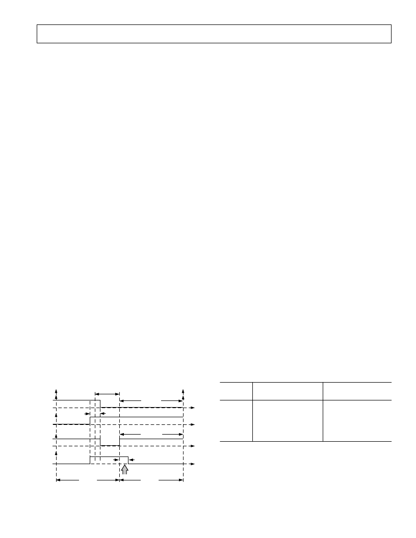
Figure 24 illustrates two examples of such transitions where in
Figure 24(a) when transitioning from normal modulation to full
ON at the half cycle boundary in double update mode, no special
action is needed. However, in Figure 24(b) when transitioning into
full OFF at the same boundary, it can be seen that an additional
dead time is necessary.
2
PWMDT
PWMCHA
1
FULL ON
AH
AL
2
PWMDT
FULL OFF
AH
AL
(a)
(b)
PWMTM
PWMTM
DEAD TIME INSERTED
Figure 24. Examples of transitioning form normal modu-
lation into either Full ON or Full OFF where it may be nec-
essary to insert additional dead times.
Minimum Pulsewidth, PWMPD Register
In many power converter switching applications, it is desirable
to eliminate PWM switching signals below a certain width. It
takes a certain finite time to both turn on and turn off power
semiconductor devices. Therefore, if the width of any of the
PWM signals goes below some minimum value, it may be desir-
able to completely eliminate the PWM switching for that par-
ticular cycle. The allowable minimum pulsewidth for any of the
six PWM outputs that can be produced by the PWM controller
may be programmed using the 10-bit PWMPD register. The
minimum pulsewidth, T
MIN
, is programmed in increments of
t
CK
as:
T
PWMPD
MIN
so that a
PWMPD
value of 0x00A defines a permissible mini-
mum on time of 0.39
μ
s for a 26 MHz CLKOUT. The opera-
tion of the minimum pulsewidth control ensures that the time
from turning ON to turning OFF (or alternatively from turning
OFF to turning ON) any PWM signal is never less than the
T
MIN
value as specified by the PWMPD register. If the PWM
controller detects that the time between turning ON and turning
OFF any one PWM signal (say AH) is less than T
MIN
, the PWM
pulse is deleted and the PWM signal remains completely OFF
over the PWM period. The complementary signal, AL in this
case, is then turned completely ON.
Effective PWM Resolution
In single update mode, the same values of PWMCHA, PWMCHB
and PWMCHC are used to define the on-times in both half
cycles of the PWM period. As a result, the effective resolution of
the PWM generation process is 2t
CK
(or 77 ns for a 26 MHz
CLKOUT), since incrementing one of the duty cycle registers
by one changes the resultant on-time of the associated PWM
signals by t
CK
in each half period (or 2t
CK
for the full period). In
double update mode, improved resolution is possible since
different values of the duty cycles registers are used to define the
on-times in both the first and second halves of the PWM period.
As a result, it is possible to adjust the on-time over the whole
period in increments of t
CK
. This corresponds to an effective
PWM resolution of t
CK
in double update mode (or 38.5 ns for a
26 MHz CLKOUT). The achievable PWM switching frequency
at a given PWM resolution is tabulated in Table IV.
t
CK
=
×
Table IV. Achievable PWM Resolution in Single and Double
Update Modes (CLKOUT = 26 MHz)
Resolution
(Bits)
Single Update Mode
PWM Frequency (kHz)
Double Update Mode
PWM Frequency (kHz)
8
9
10
11
12
50.8
25.4
12.7
6.35
3.17
102
50.8
25.4
12.7
6.35
OUTPUT CONTROL UNIT, PWMSEG REGISTER
The operation of the Output Control Unit is controlled by the
9-bit read/write PWMSEG register which controls two distinct
features that are directly useful in the control of ECM or BDCM.
Crossover Feature
The PWMSEG register contains three crossover bits; one for
each pair of PWM outputs. Setting Bit 8 of the PWMSEG regis-
ter enables the crossover mode for the AH/AL pair of PWM
相關(guān)PDF資料 |
PDF描述 |
|---|---|
| ADMC401-PB | Single-Chip, DSP-Based High Performance Motor Controller |
| ADMCF340 | DashDSPTM 64-Lead Flash Mixed-Signal DSP with Enhanced Analog Front End |
| ADMCF340BST | DashDSPTM 64-Lead Flash Mixed-Signal DSP with Enhanced Analog Front End |
| ADMCF340-EVALKIT | Circular Connector; No. of Contacts:7; Series:MS27497; Body Material:Aluminum; Connecting Termination:Crimp; Connector Shell Size:10; Circular Contact Gender:Pin; Circular Shell Style:Wall Mount Receptacle; Insert Arrangement:10-99 RoHS Compliant: No |
| ADMCF341 | DashDSP⑩ 28-Lead Flash Mixed-Signal DSP with Enhanced Analog Front End |
相關(guān)代理商/技術(shù)參數(shù) |
參數(shù)描述 |
|---|---|
| ADMC401BST | 制造商:Analog Devices 功能描述:DSP Motor Controller 144-Pin LQFP 制造商:Analog Devices 功能描述:IC MOTOR CONTROLLER |
| ADMC401BSTZ | 功能描述:IC DSP 8CH 12BIT MOTCTRL 144LQFP RoHS:是 類別:集成電路 (IC) >> 嵌入式 - DSP(數(shù)字式信號處理器) 系列:電機(jī)控制 標(biāo)準(zhǔn)包裝:2 系列:StarCore 類型:SC140 內(nèi)核 接口:DSI,以太網(wǎng),RS-232 時(shí)鐘速率:400MHz 非易失內(nèi)存:外部 芯片上RAM:1.436MB 電壓 - 輸入/輸出:3.30V 電壓 - 核心:1.20V 工作溫度:-40°C ~ 105°C 安裝類型:表面貼裝 封裝/外殼:431-BFBGA,F(xiàn)CBGA 供應(yīng)商設(shè)備封裝:431-FCPBGA(20x20) 包裝:托盤 |
| ADMC401BSTZKL1 | 制造商:Analog Devices 功能描述: |
| ADMC401-PB | 制造商:AD 制造商全稱:Analog Devices 功能描述:Single-Chip, DSP-Based High Performance Motor Controller |
| ADMCF326 | 制造商:AD 制造商全稱:Analog Devices 功能描述:28-Lead Flash Memory DSP Motor Controller |
發(fā)布緊急采購,3分鐘左右您將得到回復(fù)。