- 您現在的位置:買賣IC網 > PDF目錄374016 > ADMC401-PB (Analog Devices, Inc.) Single-Chip, DSP-Based High Performance Motor Controller PDF資料下載
參數資料
| 型號: | ADMC401-PB |
| 廠商: | Analog Devices, Inc. |
| 英文描述: | Single-Chip, DSP-Based High Performance Motor Controller |
| 中文描述: | 單芯片,基于DSP的高性能電機控制器 |
| 文件頁數: | 23/60頁 |
| 文件大小: | 417K |
| 代理商: | ADMC401-PB |
第1頁第2頁第3頁第4頁第5頁第6頁第7頁第8頁第9頁第10頁第11頁第12頁第13頁第14頁第15頁第16頁第17頁第18頁第19頁第20頁第21頁第22頁當前第23頁第24頁第25頁第26頁第27頁第28頁第29頁第30頁第31頁第32頁第33頁第34頁第35頁第36頁第37頁第38頁第39頁第40頁第41頁第42頁第43頁第44頁第45頁第46頁第47頁第48頁第49頁第50頁第51頁第52頁第53頁第54頁第55頁第56頁第57頁第58頁第59頁第60頁
ADMC401
–23–
REV. B
and BSHAN) to the inverting terminal of the two sample and
hold amplifiers (SHA) so that external signals can be correctly
biased about the nominal operating range of the ADC.
ADC0(15...0)
ADC1(15...0)
ADC2(15...0)
ADC3(15...0)
ADC4(15...0)
ADC5(15...0)
ADC6(15...0)
ADC7(15...0)
ADCXTRA(15...0)
ADCOTR(7...0)
ADCSTAT(4...0)
ADCCTRL(4...0)
MULTIPLEXER, SHA AND ADC CONTROL
INTERNAL
REFERENCE
SIGNALS
ASHAN
VIN0
VIN1
VIN2
VIN3
VIN4
VIN5
VIN6
VIN7
BSHAN
PWMSYNC
CONVST
CLKOUT
CAPT
CAPB
V
REF
REFCOM
SENSE
CML
VOLTAGE
REFERENCE
GENERATION
& CONTROL
12-BIT
PIPELINE
FLASH ADC
DATA
CONTROL SIGNALS
END OF
CONVERSION
OUT
OF
RANGE
MUX
MUX
MUX
SHA A
GAIN
SHA B
PWMSYNC (FROM PWM PERIPHERAL)
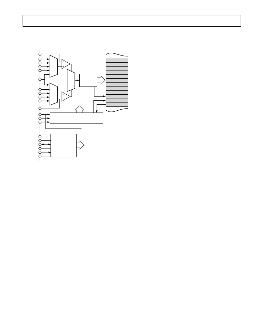
Figure 16. Functional Block Diagram of the ADC System
of the ADMC401
The basic architecture of the ADC system consists of a four-
stage pipeline architecture (the A/D core) with wideband input
sample and hold amplifiers. Excluding the last stage, each stage
of the pipeline consists of a low resolution flash A/D connected
to a switched capacitor DAC and interstage residue amplifier
(MDAC). The reside amplifier amplifies the difference between
the reconstructed DAC output and the flash input for the next
stage in the pipeline. The last stage of the pipeline simply con-
sists of a flash A/D. The pipeline architecture allows a greater
throughput rate at the expense of pipeline delay or latency. This
means that while the converter is capable of capturing a new
input sample every ADC clock cycle, it actually takes 3 1/2 ADC
clock cycles for the conversion process of any input to be fully
processed and appear at the output.
The ADC may operate in two basic conversion modes,
Simulta-
neous Sampling
or
Sequential Sampling
. The operating mode is
selected by dedicated bits in the ADCCTRL register. In the
Simultaneous Sampling
mode, two analog inputs (one from each
bank) are sampled simultaneously so that VIN0 and VIN4,
VIN1 and VIN5, VIN2 and VIN6, VIN3 and VIN7 represent
four pairs of simultaneously sampled inputs. In the alternative
sequential operating mode, there is no simultaneous sampling,
and the analog inputs are sampled and converted one after the
other (i.e., VIN0 followed by VIN1 followed by VIN2, etc.). In
this mode, successive analog inputs are sampled an ADC clock
period (or four DSP clock cycles) apart.
The conversion sequence may be initiated either internally (syn-
chronized to the PWM generation) or from an external event on
the CONVST pin. In the default
Simultaneous Sampling
mode of
operation, the internal control logic simultaneously samples the
first pair of input signals (VIN0 and VIN4) following the con-
vert start command. Subsequently, these inputs are multiplexed
into the 12-bit analog-to-digital converter. After a delay of two
ADC clock cycles, the second pair of analog inputs (VIN1 and
VIN5) are sampled simultaneously and then multiplexed into
the ADC. This process continues until all four pairs of analog
inputs have been sampled and converted. As the conversion for
a given analog input channel is completed, the corresponding
digital number is written to a dedicated 16-bit, twos comple-
ment, left-aligned register that is memory mapped to the data
memory space of the DSP core. The ADC data register ADC0
stores the conversion result for the signal on VIN0, etc.
Following the end of conversion of each pair of analog inputs, a
dedicated bit is set in the ADCSTAT register. The result of this
highly efficient pipelined structure is that all eight ADC data
registers will contain valid conversion results less than 2
μ
s (at
26 MHz) after the convert start command. At this point a dedi-
cated ADC interrupt will be generated. Alternatively, if data is
required sooner, the ADCSTAT register can be polled to detect
when a given pair of analog inputs have been successfully con-
verted, except in
Sequential
Sampling
mode.
Once the conversion sequence has been completed and all eight
ADC data registers have been updated, the entire ADC structure
automatically reverts to the
Single Channel
mode and continu-
ously converts the analog input on the VIN0 pin. The results of
this conversion are placed in the additional ADCXTRA register
and are updated once every ADC clock cycle. This feature could
be used to continuously monitor a single analog input on the
VIN0 pin.
There are two additional modes of operation of the ADC system
that may be used for offset and gain calibration of the entire
system. In the
Offset Calibration
mode, all analog inputs (VIN0
to VIN7, GAIN, ASHAN and BSHAN) are disconnected from
the inputs to the sample and hold amplifiers. Instead, both
terminals of each sample and hold amplifiers are connected
together and to the voltage reference. Following a conversion
sequence, the data in the ADC data register can be taken as a
measure of any offset in the sample and hold amplifiers and
ADC. Additionally, in the
Gain Calibration
mode, the dedicated
analog input GAIN is applied to the noninverting terminal of
both sample and hold amplifiers. Any number of precise exter-
nal voltages can be applied to this pin to measure and correct
for any gain errors, if required.
Along with each data output from the A/D converter, an Out-of-
Range (OTR) bit is set if the signal exceeds the permissible
input voltage span. In normal conversion, the eight OTR bits for
the eight analog inputs are stored in the ADCOTR register, with
one bit for each analog input. The OTR bit for the ADCXTRA
register is stored in the ADCSTAT register.
The ADC may use either an internally generated 2.0 V precision
reference voltage or an externally supplied reference voltage
level at the V
REF
pin. The operating mode is selected by the
connection of the SENSE pin.
相關PDF資料 |
PDF描述 |
|---|---|
| ADMCF340 | DashDSPTM 64-Lead Flash Mixed-Signal DSP with Enhanced Analog Front End |
| ADMCF340BST | DashDSPTM 64-Lead Flash Mixed-Signal DSP with Enhanced Analog Front End |
| ADMCF340-EVALKIT | Circular Connector; No. of Contacts:7; Series:MS27497; Body Material:Aluminum; Connecting Termination:Crimp; Connector Shell Size:10; Circular Contact Gender:Pin; Circular Shell Style:Wall Mount Receptacle; Insert Arrangement:10-99 RoHS Compliant: No |
| ADMCF341 | DashDSP⑩ 28-Lead Flash Mixed-Signal DSP with Enhanced Analog Front End |
| ADMCF341BR | DashDSP⑩ 28-Lead Flash Mixed-Signal DSP with Enhanced Analog Front End |
相關代理商/技術參數 |
參數描述 |
|---|---|
| ADMCF326 | 制造商:AD 制造商全稱:Analog Devices 功能描述:28-Lead Flash Memory DSP Motor Controller |
| ADMCF326BN | 制造商:Analog Devices 功能描述: |
| ADMCF326BR | 制造商:AD 制造商全稱:Analog Devices 功能描述:28-Lead Flash Memory DSP Motor Controller |
| ADMCF326BRZ | 制造商:Rochester Electronics LLC 功能描述: 制造商:Analog Devices 功能描述: |
| ADMCF326BRZ-REEL | 制造商:Rochester Electronics LLC 功能描述: 制造商:Analog Devices 功能描述: |
發布緊急采購,3分鐘左右您將得到回復。