- 您現在的位置:買賣IC網 > PDF目錄374016 > ADMCF341-EVALKIT (Analog Devices, Inc.) DashDSP⑩ 28-Lead Flash Mixed-Signal DSP with Enhanced Analog Front End PDF資料下載
參數資料
| 型號: | ADMCF341-EVALKIT |
| 廠商: | Analog Devices, Inc. |
| 英文描述: | DashDSP⑩ 28-Lead Flash Mixed-Signal DSP with Enhanced Analog Front End |
| 中文描述: | DashDSP⑩28引腳閃存混合信號增強的DSP與模擬前端 |
| 文件頁數: | 14/36頁 |
| 文件大小: | 1106K |
| 代理商: | ADMCF341-EVALKIT |
第1頁第2頁第3頁第4頁第5頁第6頁第7頁第8頁第9頁第10頁第11頁第12頁第13頁當前第14頁第15頁第16頁第17頁第18頁第19頁第20頁第21頁第22頁第23頁第24頁第25頁第26頁第27頁第28頁第29頁第30頁第31頁第32頁第33頁第34頁第35頁第36頁
REV. 0
–14–
ADMCF341
PWMSYNC
AH
AL
PWMCHA
PWMCHA
2
PWMDT
PWMSYNCWT + 1
2
PWMDT
SYSSTAT (3)
PWMTM
PWMTM
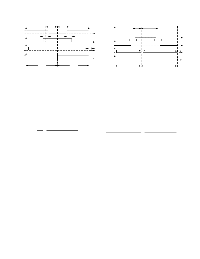
Figure 7. Typical PWM Outputs of Three-Phase
Timing Unit in Single Update Mode
Each switching edge is moved by an equal amount (PWMDT
t
CK
) to preserve the symmetrical output patterns. The
PWMSYNC pulse, whose width is set by the PWMSYNCWT
register, is also shown. Bit 3 of the SYSSTAT register indicates
which half cycle is active. This can be useful in double update
mode, as will be discussed later.
The resultant on-times of the PWM signals shown in Figure 7
may be written as:
=
2 (
=
2 (
The corresponding duty cycles are:
T
PWMCHA
PWMDT
t
AH
CK
-
¥
)
T
PWMTM
PWMCHA
PWMDT
t
AL
CK
-
-
¥
)
d
T
T
PWMCHA
PWMDT
PWMTM
AH
AH
S
=
=
-
d
T
T
PWMTM
PWMCHA
PWMTM
PWMDT
AL
AL
S
=
=
-
-
Obviously, negative values of
T
AH
and
T
AL
are not permitted
because the minimum permissible value is zero, corresponding
to a 0% duty cycle. In a similar fashion, the maximum value is
T
S
, corresponding to a 100% duty cycle.
The output signals from the timing unit for operation in double
update mode are shown in Figure 8. This illustrates a com-
pletely general case where the switching frequency, dead time,
and duty cycle are all changed in the second half of the PWM
period. Of course, the same value for any or all of these quanti-
ties could be used in both halves of the PWM cycle. However, it
can be seen that there is no guarantee that symmetrical PWM
signals will be produced by the timing unit in this double update
mode. Additionally, it is seen that the dead time is inserted into
the PWM signals in the same way as in single update mode.
PWMCHA
2
2
PWMDT
1
2
PWMDT
2
PWMSYNCWT
2
+ 1
PWMCHA
1
PWMTM
1
PWMTM
2
PWMSYNCWT
1
+ 1
AH
AL
PWMSYNC
SYSSTAT (3)
Figure 8.
Typical PWM Outputs of Three-Phase
Timing Unit in Double Update Mode
In general, the on-times of the PWM signals in double update
mode are defined by:
T
(
PWMCHA
PWMDT
PWMCHA
PWMDT
T
AH
CK
=
+
-
-
¥
)
1
2
1
2
T
(
PWMTM
PWMCHA
PWMTM
PWMDT
-
PWMCHA
PWMDT
t
AL
CK
=
+
-
-
-
¥
)
1
2
1
2
1
2
d
T
T
PWMCHA
PWMTM
PWMCHA
PWMTM
PWMDT
PWMTM
PWMDT
PWMTM
AH
AH
S
=
=
+
+
-
+
+
1
2
1
2
1
2
1
2
d
T
T
PWMTM
PWMTM
PWMCHA
PWMTM
PWMTM
PWMCHA
PWMDT
+
1
PWMCHA
PWMTM
PWMTM
AL
AL
S
=
=
+
+
+
-
+
+
1
2
1
1
2
2
1
1
2
because for the completely general case in double update mode,
the switching period is given by:
=
(
1
Again, the values of
T
AH
and
T
AL
are constrained to lie between
zero and
T
S
.
PWM signals similar to those illustrated in Figure 7 and Figure 8
can be produced on the BH, BL, CH, and CL outputs by
programming the PWMCHB and PWMCHC registers in a
manner identical to that described for PWMCHA.
The PWM controller does not produce any PWM outputs until
all of the PWMTM, PWMCHA, PWMCHB, and PWMCHC
registers have been written to at least once. After these registers
have been written, the counters in the three-phase timing unit
are enabled. Writing to these registers also starts the main PWM
timer. If, during initialization, the PWMTM register is written
before the PWMCHA, PWMCHB, and PWMCHC registers,
the first PWMSYNC pulse (and interrupt if enabled) will be
generated (1.5
¥
t
CK
¥
PWMTM) seconds after the initial write
to the PWMTM register in single update mode. In double up-
date mode, the first PWMSYNC pulse will be generated (t
CK
¥
PWMTM) seconds after the initial write to the PWMTM regis-
ter in single update mode.
T
PWMTM
PWMTM
t
S
CK
+
¥
)
2
相關PDF資料 |
PDF描述 |
|---|---|
| ADN2811 | OC-48/OC-48 FEC Clock and Data Recovery IC with Integrated Limiting Amp |
| ADN2811ACP-CML | OC-48/OC-48 FEC Clock and Data Recovery IC with Integrated Limiting Amp |
| ADN2811ACP-CML-RL | OC-48/OC-48 FEC Clock and Data Recovery IC with Integrated Limiting Amp |
| ADN2812 | Continuous Rate 12.3 Mb/s to 2.7 Gb/s Clock and Data Recovery IC with Integrated Limiting Amp |
| ADN2812ACP | Continuous Rate 12.3 Mb/s to 2.7 Gb/s Clock and Data Recovery IC with Integrated Limiting Amp |
相關代理商/技術參數 |
參數描述 |
|---|---|
| AD-MCX-RPSMAF | 功能描述:ADAPTER AU RPSMA FEM-MCX APPLE RoHS:是 類別:RF/IF 和 RFID >> RF配件 系列:* 標準包裝:1 系列:* |
| AD-MD3FF | 制造商:Pan Pacific 功能描述: |
| AD-MD4FF | 制造商:Pan Pacific 功能描述: |
| AD-MD6F/D5M | 制造商:Pan Pacific 功能描述: |
| AD-MD6FF | 制造商:Pan Pacific 功能描述: |
發布緊急采購,3分鐘左右您將得到回復。