- 您現(xiàn)在的位置:買賣IC網(wǎng) > PDF目錄374016 > ADMCF341-EVALKIT (Analog Devices, Inc.) DashDSP⑩ 28-Lead Flash Mixed-Signal DSP with Enhanced Analog Front End PDF資料下載
參數(shù)資料
| 型號: | ADMCF341-EVALKIT |
| 廠商: | Analog Devices, Inc. |
| 英文描述: | DashDSP⑩ 28-Lead Flash Mixed-Signal DSP with Enhanced Analog Front End |
| 中文描述: | DashDSP⑩28引腳閃存混合信號增強(qiáng)的DSP與模擬前端 |
| 文件頁數(shù): | 18/36頁 |
| 文件大小: | 1106K |
| 代理商: | ADMCF341-EVALKIT |
第1頁第2頁第3頁第4頁第5頁第6頁第7頁第8頁第9頁第10頁第11頁第12頁第13頁第14頁第15頁第16頁第17頁當(dāng)前第18頁第19頁第20頁第21頁第22頁第23頁第24頁第25頁第26頁第27頁第28頁第29頁第30頁第31頁第32頁第33頁第34頁第35頁第36頁
REV. 0
–18–
ADMCF341
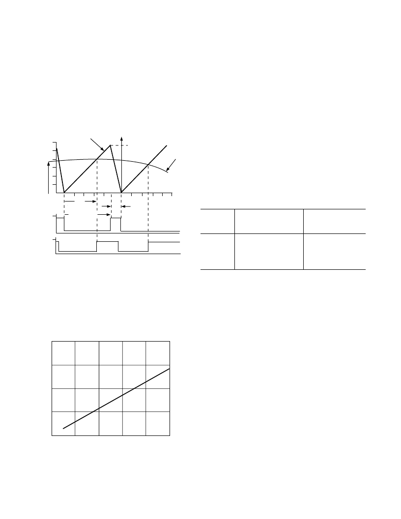
Following reset, VC = 0 at t = 0. This reset and the start of the
conversion process are initiated by the PWMSYNC pulse, as
shown in Figure 12. The width of the PWMSYNC pulse is
controlled by the PWMSYNCWT register and should be pro-
grammed according to Figure 13 to ensure complete resetting.
In order to compensate for IC process manufacturing tolerances
(and to adjust for capacitor tolerances), the current source of
the ADMCF341 is software-programmable. Using software to
set the magnitude of the ICONST current generator is accom-
plished by selecting one of eight steps over approximately 20%
current range.
V
C
V1
PWMSYNC
COMPARATOR
OUTPUT
V
CMAX
T
VIL
T
PWM
– T
CRST
T
CRST
Figure 12. Analog Input Block Operation
The ADC system consists of four comparators and a single
timer, which may be clocked at either the DSP rate or half the
DSP rate, depending on the setting of the ADCCNT bit (bit 7)
of the MODECTRL register. When this bit is cleared, the timer
counts at a slower rate of CLKIN. When this bit is set, it counts
at CLKOUT or twice the rate of CLKIN. ADC1, ADC2,
ADC3, and ADCAUX are the registers that capture the conver-
sion times, which are the timer values when the associated
comparator trips.
200
150
100
50
0
0 2 4 6 8 10
D
CHARGING CAPACITOR – nF
Figure 13. PWMSYNCWT Program Value
ADC Resolution
The ADC is intrinsically linked to the PWM block through the
PWMSYNC pulse’s control of the ADC conversion process.
Because of this link, the effective resolution of the ADC is a
function of both the PWM switching frequency and the rate at
which the ADC counter timer is clocked. For a CLKOUT
period of t
CK
and a PWM period of T
PWM
, the maximum count
of the ADC is given by:
Max Count
T
T
=
-
7
t
for MODECTRL Bit
Max Count
for MODECTRL Bit
T
T
=
t
PWM
CRST
0
CK
PWM
CRST
1
CK
=
-
7
=
min
min
(
,(
)/
)
(
,(
)/
)
4095
2
4095
where T
PWM
is equal to the PWM period if operating in single
update mode or equal to half that period if operating in
double update mode. For an assumed CLKOUT frequency
of 20 MHz and PWMSYNC pulsewidth of 2.0
m
s, the effec-
tive resolution of the ADC block is tabulated for various
PWM switching frequencies in Table VII.
Table VII. ADC Resolution Examples
PWM
Frequency
(kHz)
2.4
4
8
18
25
MODECTRL[7] = 0
Max
Effective
Count
Resolution
4095
12
2480
>11
1230
>10
535
>9
380
>8
MODECTRL[7] = 1
Max
Effective
Count
Resolution
4095
12
4095
12
2460
>11
1070
>10
760
>9
Programmable Current Source
The ADMCF341 has an internal current source that is used to
charge an external capacitor, generating the voltage ramp used
for conversion. The magnitude of the output of the current
source circuit is subject to manufacturing variations and can
vary from one device to the next. Therefore, the ADMCF341
includes a programmable current source whose output can
always be tuned to within 5% of the target 100
m
A. A 3-bit
register, I
CONST
_TRIM, allows the user to make this adjust-
ment. The output current is proportional to the value written to
the register: 0x0 produces the minimum output and 0x7 pro-
duces the maximum output. The default value of I
CONST
_TRIM
after reset is 0x0.
Charging Capacitor Selection
The charging capacitor value is selected based on the sample
(PWM) frequency desired. A too-small capacitor value will re-
duce the available resolution of the ADC by having the ramp
voltage rise rapidly and convert too quickly, not utilizing all pos-
sible counts available in the PWM cycle. A too-large capacitor
may not convert in the available PWM cycle returning 0x000.
To select a charging capacitor use Figure 14. Select the sam-
pling frequency desired, determine if the current source is to be
tuned to a nominal 100
m
A or left in the default (0x0 code) trim
state, then determine the proper charge capacitor off the appro-
priate curve.
相關(guān)PDF資料 |
PDF描述 |
|---|---|
| ADN2811 | OC-48/OC-48 FEC Clock and Data Recovery IC with Integrated Limiting Amp |
| ADN2811ACP-CML | OC-48/OC-48 FEC Clock and Data Recovery IC with Integrated Limiting Amp |
| ADN2811ACP-CML-RL | OC-48/OC-48 FEC Clock and Data Recovery IC with Integrated Limiting Amp |
| ADN2812 | Continuous Rate 12.3 Mb/s to 2.7 Gb/s Clock and Data Recovery IC with Integrated Limiting Amp |
| ADN2812ACP | Continuous Rate 12.3 Mb/s to 2.7 Gb/s Clock and Data Recovery IC with Integrated Limiting Amp |
相關(guān)代理商/技術(shù)參數(shù) |
參數(shù)描述 |
|---|---|
| AD-MCX-RPSMAF | 功能描述:ADAPTER AU RPSMA FEM-MCX APPLE RoHS:是 類別:RF/IF 和 RFID >> RF配件 系列:* 標(biāo)準(zhǔn)包裝:1 系列:* |
| AD-MD3FF | 制造商:Pan Pacific 功能描述: |
| AD-MD4FF | 制造商:Pan Pacific 功能描述: |
| AD-MD6F/D5M | 制造商:Pan Pacific 功能描述: |
| AD-MD6FF | 制造商:Pan Pacific 功能描述: |
發(fā)布緊急采購,3分鐘左右您將得到回復(fù)。