- 您現(xiàn)在的位置:買賣IC網(wǎng) > PDF目錄374016 > ADN2812ACP-RL (ANALOG DEVICES INC) Continuous Rate 12.3 Mb/s to 2.7 Gb/s Clock and Data Recovery IC with Integrated Limiting Amp PDF資料下載
參數(shù)資料
| 型號: | ADN2812ACP-RL |
| 廠商: | ANALOG DEVICES INC |
| 元件分類: | 數(shù)字傳輸電路 |
| 英文描述: | Continuous Rate 12.3 Mb/s to 2.7 Gb/s Clock and Data Recovery IC with Integrated Limiting Amp |
| 中文描述: | CLOCK RECOVERY CIRCUIT, QCC32 |
| 封裝: | 5 X 5 MM, MO-220VHHD-2, LFCSP-32 |
| 文件頁數(shù): | 13/28頁 |
| 文件大小: | 478K |
| 代理商: | ADN2812ACP-RL |
第1頁第2頁第3頁第4頁第5頁第6頁第7頁第8頁第9頁第10頁第11頁第12頁當前第13頁第14頁第15頁第16頁第17頁第18頁第19頁第20頁第21頁第22頁第23頁第24頁第25頁第26頁第27頁第28頁
ADN2812
JITTER SPECIFICATIONS
The ADN2812 CDR is designed to achieve the best bit-error-
rate (BER) performance and exceeds the jitter transfer, genera-
tion, and tolerance specifications proposed for SONET/SDH
equipment defined in the Telcordia Technologies specification.
Rev. 0 | Page 13 of 28
Jitter is the dynamic displacement of digital signal edges from
their long-term average positions, measured in unit intervals
(UI), where 1 UI = 1 bit period. Jitter on the input data can
cause dynamic phase errors on the recovered clock sampling
edge. Jitter on the recovered clock causes jitter on the
retimed data.
The following sections briefly summarize the specifications of
jitter generation, transfer, and tolerance in accordance with the
Telcordia document (GR-253-CORE, Issue 3, September 2000)
for the optical interface at the equipment level and the
ADN2812 performance with respect to those specifications.
JITTER GENERATION
The jitter generation specification limits the amount of jitter
that can be generated by the device with no jitter and wander
applied at the input. For OC-48 devices, the band-pass filter
has a 12 kHz high-pass cutoff frequency with a roll-off of
20 dB/decade, and a low-pass cutoff frequency of at least
20 MHz. The jitter generated must be less than 0.01 UI rms, and
must be less than 0.1 UI p-p.
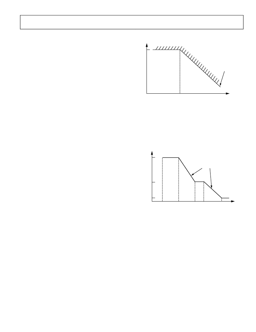
JITTER TRANSFER
The jitter transfer function is the ratio of the jitter on the output
signal to the jitter applied on the input signal versus the
frequency. This parameter measures the limited amount of the
jitter on an input signal that can be transferred to the output
signal (see Figure 15).
0
0.1
ACCEPTABLE
RANGE
f
C
JITTER FREQUENCY (kHz)
SLOPE = –20dB/DECADE
J
Figure 15. Jitter Transfer Curve
JITTER TOLERANCE
The jitter tolerance is defined as the peak-to-peak amplitude of
the sinusoidal jitter applied on the input signal, which causes a
1 dB power penalty. This is a stress test intended to ensure that
no additional penalty is incurred under the operating
conditions (see Figure 16).
0
15.00
1.50
0.15
f
0
f
1
f
2
f
3
f
4
JITTER FREQUENCY (kHz)
SLOPE = –20dB/DECADE
I
Figure 16. SONET Jitter Tolerance Mask
相關PDF資料 |
PDF描述 |
|---|---|
| ADN2812ACP-RL7 | Continuous Rate 12.3 Mb/s to 2.7 Gb/s Clock and Data Recovery IC with Integrated Limiting Amp |
| ADN2819 | Multirate to 2.7 Gb/s Clock and Data Recovery IC with Integrated Limiting Amp |
| ADN2819ACP-CML | Multirate to 2.7 Gb/s Clock and Data Recovery IC with Integrated Limiting Amp |
| ADN2819ACP-CML-RL | Multirate to 2.7 Gb/s Clock and Data Recovery IC with Integrated Limiting Amp |
| ADN2819ACPZ-CML-RL1 | Multirate to 2.7 Gb/s Clock and Data Recovery IC with Integrated Limiting Amp |
相關代理商/技術參數(shù) |
參數(shù)描述 |
|---|---|
| ADN2812ACP-RL7 | 制造商:Analog Devices 功能描述:Clock and Data Recovery 32-Pin LFCSP EP T/R |
| ADN2812ACPZ | 功能描述:IC CLOCK/DATA RECOVERY 32LFCSP RoHS:是 類別:集成電路 (IC) >> 時鐘/計時 - 專用 系列:- 標準包裝:1 系列:- 類型:時鐘/頻率發(fā)生器,多路復用器 PLL:是 主要目的:存儲器,RDRAM 輸入:晶體 輸出:LVCMOS 電路數(shù):1 比率 - 輸入:輸出:1:2 差分 - 輸入:輸出:無/是 頻率 - 最大:400MHz 電源電壓:3 V ~ 3.6 V 工作溫度:0°C ~ 85°C 安裝類型:表面貼裝 封裝/外殼:16-TSSOP(0.173",4.40mm 寬) 供應商設備封裝:16-TSSOP 包裝:Digi-Reel® 其它名稱:296-6719-6 |
| ADN2812ACPZ-RL | 功能描述:IC CLOCK/DATA RECOVERY 32LFCSP RoHS:是 類別:集成電路 (IC) >> 時鐘/計時 - 專用 系列:- 標準包裝:28 系列:- 類型:時鐘/頻率發(fā)生器 PLL:是 主要目的:Intel CPU 服務器 輸入:時鐘 輸出:LVCMOS 電路數(shù):1 比率 - 輸入:輸出:3:22 差分 - 輸入:輸出:無/是 頻率 - 最大:400MHz 電源電壓:3.135 V ~ 3.465 V 工作溫度:0°C ~ 85°C 安裝類型:表面貼裝 封裝/外殼:64-TFSOP (0.240",6.10mm 寬) 供應商設備封裝:64-TSSOP 包裝:管件 |
| ADN2812ACPZ-RL7 | 功能描述:IC CLOCK/DATA RECOVERY 32LFCSP RoHS:是 類別:集成電路 (IC) >> 時鐘/計時 - 專用 系列:- 標準包裝:28 系列:- 類型:時鐘/頻率發(fā)生器 PLL:是 主要目的:Intel CPU 服務器 輸入:時鐘 輸出:LVCMOS 電路數(shù):1 比率 - 輸入:輸出:3:22 差分 - 輸入:輸出:無/是 頻率 - 最大:400MHz 電源電壓:3.135 V ~ 3.465 V 工作溫度:0°C ~ 85°C 安裝類型:表面貼裝 封裝/外殼:64-TFSOP (0.240",6.10mm 寬) 供應商設備封裝:64-TSSOP 包裝:管件 |
| ADN2813 | 制造商:AD 制造商全稱:Analog Devices 功能描述:Continuous Rate 10 Mb/s to 1.25 Gb/s Clock and Data Recovery IC with Integrated Limiting Amp |
發(fā)布緊急采購,3分鐘左右您將得到回復。