- 您現在的位置:買賣IC網 > PDF目錄374016 > ADN2812ACP-RL (ANALOG DEVICES INC) Continuous Rate 12.3 Mb/s to 2.7 Gb/s Clock and Data Recovery IC with Integrated Limiting Amp PDF資料下載
參數資料
| 型號: | ADN2812ACP-RL |
| 廠商: | ANALOG DEVICES INC |
| 元件分類: | 數字傳輸電路 |
| 英文描述: | Continuous Rate 12.3 Mb/s to 2.7 Gb/s Clock and Data Recovery IC with Integrated Limiting Amp |
| 中文描述: | CLOCK RECOVERY CIRCUIT, QCC32 |
| 封裝: | 5 X 5 MM, MO-220VHHD-2, LFCSP-32 |
| 文件頁數: | 21/28頁 |
| 文件大小: | 478K |
| 代理商: | ADN2812ACP-RL |
第1頁第2頁第3頁第4頁第5頁第6頁第7頁第8頁第9頁第10頁第11頁第12頁第13頁第14頁第15頁第16頁第17頁第18頁第19頁第20頁當前第21頁第22頁第23頁第24頁第25頁第26頁第27頁第28頁
ADN2812
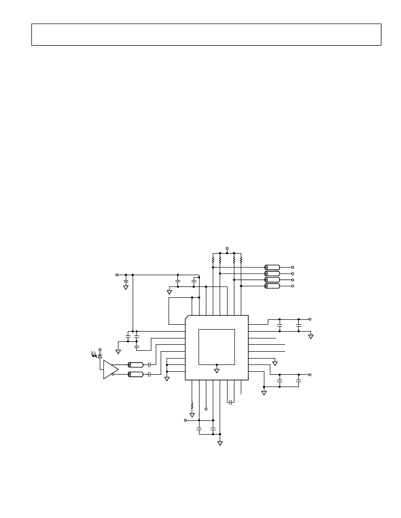
APPLICATIONS INFORMATION
PCB DESIGN GUIDELINES
Proper RF PCB design techniques must be used for optimal
performance.
Power Supply Connections and Ground Planes
Use of one low impedance ground plane is recommended. The
VEE pins should be soldered directly to the ground plane to
reduce series inductance. If the ground plane is an internal
plane and connections to the ground plane are made through
vias, multiple vias can be used in parallel to reduce the series
inductance, especially on Pin 23, which is the ground return for
the output buffers. The exposed pad should be connected to the
GND plane using plugged vias
so that solder does not leak
through the vias during reflow.
Rev. 0 | Page 21 of 28
Use of a 10 μF electrolytic capacitor between VCC and VEE is
recommended at the location where the 3.3 V supply enters the
PCB. When using 0.1 μF and 1 nF ceramic chip capacitors, they
should be placed between the IC power supply VCC and VEE,
as close as possible to the ADN2812 VCC pins.
If connections to the supply and ground are made through vias,
the use of multiple vias in parallel helps to reduce series
inductance, especially on Pin 24, which supplies power to the
high speed CLKOUTP/CLKOUTN and DATAOUTP/
DATAOUTN output buffers. Refer to the schematic in Figure 24
for recommended connections.
By using adjacent power supply and GND planes, excellent high
frequency decoupling can be realized by using close spacing
between the planes. This capacitance is given by
(
)
pF
ε
88
.
A/d
C
r
plane
=
where:
ε
r
is the dielectric constant of the PCB material.
A
is the area of the overlap of power and GND planes (cm
2
).
d
is the separation between planes (mm).
For FR-4,
ε
r
= 4.4 mm and 0.25 mm spacing,
C
~15 pF/cm
2
.
0
R
TH
NC
NC = NO CONNECT
1
2
3
4
5
6
7
8
TEST1
VCC
VREF
NIN
PIN
SLICEP
SLICEN
VEE
VCC
50
TRANSMISSION LINES
100
×
4
VCC
VEE
LOS
SDA
SCK
SADDR5
VCC
VEE
T
V
V
D
D
S
C
C
T
R
R
V
V
C
C
L
9
10 11 12 13 14 15 16
32 31 30 29 28 27 26 25
24
23
22
21
20
19
18
17
EXPOSED PAD
TIED OFF TO
VEE PLANE
WITH VIAS
CLKOUTN
CLKOUTP
DATAOUTN
DATAOUTP
VCC
TIA
50
50
C
IN
C
IN
1nF
0.1
μ
F
0.1
μ
F
10
μ
F+
0.1
μ
F
1nF
VCC
VCC
VCC
μ
C
μ
C
I
2
C
CONTROLLER
0.1
μ
F
1nF
0.1
μ
F
VCC
1nF
0.1
μ
F
0.47
μ
F
±
20% >300M
INSULATION RESISTANCE
1nF
Figure 24. Typical ADN2812 Applications Circuit
相關PDF資料 |
PDF描述 |
|---|---|
| ADN2812ACP-RL7 | Continuous Rate 12.3 Mb/s to 2.7 Gb/s Clock and Data Recovery IC with Integrated Limiting Amp |
| ADN2819 | Multirate to 2.7 Gb/s Clock and Data Recovery IC with Integrated Limiting Amp |
| ADN2819ACP-CML | Multirate to 2.7 Gb/s Clock and Data Recovery IC with Integrated Limiting Amp |
| ADN2819ACP-CML-RL | Multirate to 2.7 Gb/s Clock and Data Recovery IC with Integrated Limiting Amp |
| ADN2819ACPZ-CML-RL1 | Multirate to 2.7 Gb/s Clock and Data Recovery IC with Integrated Limiting Amp |
相關代理商/技術參數 |
參數描述 |
|---|---|
| ADN2812ACP-RL7 | 制造商:Analog Devices 功能描述:Clock and Data Recovery 32-Pin LFCSP EP T/R |
| ADN2812ACPZ | 功能描述:IC CLOCK/DATA RECOVERY 32LFCSP RoHS:是 類別:集成電路 (IC) >> 時鐘/計時 - 專用 系列:- 標準包裝:1 系列:- 類型:時鐘/頻率發生器,多路復用器 PLL:是 主要目的:存儲器,RDRAM 輸入:晶體 輸出:LVCMOS 電路數:1 比率 - 輸入:輸出:1:2 差分 - 輸入:輸出:無/是 頻率 - 最大:400MHz 電源電壓:3 V ~ 3.6 V 工作溫度:0°C ~ 85°C 安裝類型:表面貼裝 封裝/外殼:16-TSSOP(0.173",4.40mm 寬) 供應商設備封裝:16-TSSOP 包裝:Digi-Reel® 其它名稱:296-6719-6 |
| ADN2812ACPZ-RL | 功能描述:IC CLOCK/DATA RECOVERY 32LFCSP RoHS:是 類別:集成電路 (IC) >> 時鐘/計時 - 專用 系列:- 標準包裝:28 系列:- 類型:時鐘/頻率發生器 PLL:是 主要目的:Intel CPU 服務器 輸入:時鐘 輸出:LVCMOS 電路數:1 比率 - 輸入:輸出:3:22 差分 - 輸入:輸出:無/是 頻率 - 最大:400MHz 電源電壓:3.135 V ~ 3.465 V 工作溫度:0°C ~ 85°C 安裝類型:表面貼裝 封裝/外殼:64-TFSOP (0.240",6.10mm 寬) 供應商設備封裝:64-TSSOP 包裝:管件 |
| ADN2812ACPZ-RL7 | 功能描述:IC CLOCK/DATA RECOVERY 32LFCSP RoHS:是 類別:集成電路 (IC) >> 時鐘/計時 - 專用 系列:- 標準包裝:28 系列:- 類型:時鐘/頻率發生器 PLL:是 主要目的:Intel CPU 服務器 輸入:時鐘 輸出:LVCMOS 電路數:1 比率 - 輸入:輸出:3:22 差分 - 輸入:輸出:無/是 頻率 - 最大:400MHz 電源電壓:3.135 V ~ 3.465 V 工作溫度:0°C ~ 85°C 安裝類型:表面貼裝 封裝/外殼:64-TFSOP (0.240",6.10mm 寬) 供應商設備封裝:64-TSSOP 包裝:管件 |
| ADN2813 | 制造商:AD 制造商全稱:Analog Devices 功能描述:Continuous Rate 10 Mb/s to 1.25 Gb/s Clock and Data Recovery IC with Integrated Limiting Amp |
發布緊急采購,3分鐘左右您將得到回復。