- 您現(xiàn)在的位置:買賣IC網(wǎng) > PDF目錄374017 > ADN2847 (Analog Devices, Inc.) 3 V Dual-Loop 50 Mbps to 3.3 Gbps Laser Diode Driver PDF資料下載
參數(shù)資料
| 型號: | ADN2847 |
| 廠商: | Analog Devices, Inc. |
| 英文描述: | 3 V Dual-Loop 50 Mbps to 3.3 Gbps Laser Diode Driver |
| 中文描述: | 3伏雙回路50 Mbps至3.3 Gbps的激光二極管驅(qū)動器 |
| 文件頁數(shù): | 3/12頁 |
| 文件大小: | 1037K |
| 代理商: | ADN2847 |
REV. 0
ADN2847
–3–
Parameter
Min
Typ
Max
Unit
Conditions/Comments
SUPPLY
I
CC7
V
CC8
50
3.3
mA
V
I
BIAS
= I
MOD
= 0
3.0
3.6
NOTES
1
Temperature range: –40
∞
C to +85
∞
C.
2
The high speed performance for the die version of ADN2847 can be achieved when using the bonding diagram shown in Figure 3.
3
Measured into a 25
W
load using a 11110000 pattern at 2.5 Gbps.
4
When the voltage on DATAP is greater than the voltage on DATAN, the modulation current flows in the IMODP pin.
5
Guaranteed by design and characterization. Not production tested.
6
IDTONE may cause eye distortion.
7
I
for power calculation on page 8 is the typical I
CC
given.
8
All V
CC
pins should be shorted together.
Specifications subject to change without notice.
ABSOLUTE MAXIMUM RATINGS
1
(T
A
= 25
∞
C, unless otherwise noted.)
V
CC
to GND . . . . . . . . . . . . . . . . . . . . . . . . . . . . . . . . . . 4.2 V
Digital Inputs (ALS, LBWSET, CLKSEL) . .–0.3 V to V
CC
+ 0.3 V
IMODN, IMODP . . . . . . . . . . . . . . . . . . . . . . . . . V
CC
+ 1.2 V
Operating Temperature Range
Industrial . . . . . . . . . . . . . . . . . . . . . . . . . . .–40
∞
C to +85
∞
C
Storage Temperature Range . . . . . . . . . . . . .–65
∞
C to +150
∞
C
Junction Temperature (T
J
max) . . . . . . . . . . . . . . . . . . . 150
∞
C
48-Lead LFCSP Package
Power Dissipation
2
. . . . . . . . . . . . . . . . (T
J
max – T
A
)/
q
JA
W
q
JA
Thermal Impedance
3
. . . . . . . . . . . . . . . . . . . . . 25
∞
C/W
Lead Temperature (Soldering 10 sec) . . . . . . . . . . . . 300
∞
C
32-Lead LFCSP Package
Power Dissipation
2
. . . . . . . . . . . . . . . . (T
J
max – T
A
)/
q
JA
W
q
JA
Thermal Impedance
3
. . . . . . . . . . . . . . . . . . . . . 32
∞
C/W
Lead Temperature (Soldering 10 sec) . . . . . . . . . . . . 300
∞
C
NOTES
1
Stresses above those listed under Absolute Maximum Ratings may cause perma-
nent damage to the device. This is a stress rating only; functional operation of the
device at these or any other conditions above those listed in the operational
sections of this specification is not implied. Exposure to absolute maximum rating
conditions for extended periods may affect device reliability.
2
Power consumption formulae are provided on page 8.
3
q
JA
is defined when part is soldered on a 4-layer board.
CAUTION
ESD (electrostatic discharge) sensitive device. Electrostatic charges as high as 4000 V readily
accumulate on the human body and test equipment and can discharge without detection. Although the
ADN2847 features proprietary ESD protection circuitry, permanent damage may occur on devices
subjected to high energy electrostatic discharges. Therefore, proper ESD precautions are recommended
to avoid performance degradation or loss of functionality.
ORDERING GUIDE
Temperature
Range
Package
Description
Model
ADN2847ACP-32
ADN2847ACP-48
ADN2847ACP-32-RL
ADN2847ACP-32-RL7
ADN2847ACP-48-RL
–40
∞
C to +85
∞
C
–40
∞
C to +85
∞
C
–40
∞
C to +85
∞
C
–40
∞
C to +85
∞
C
–40
∞
C to +85
∞
C
32-Lead LFCSP
48-Lead LFCSP
32-Lead LFCSP
32-Lead LFCSP
48-Lead LFCSP
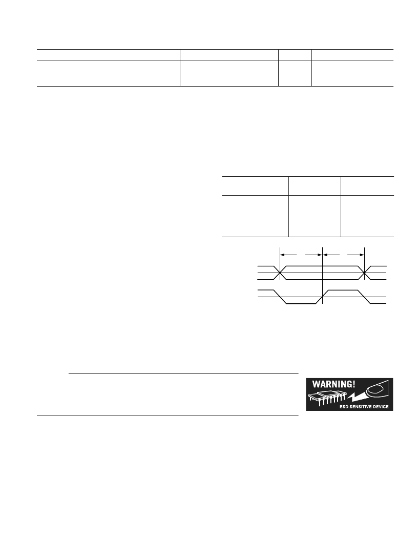
DATAP/DATAN
SETUP
t
S
HOLD
t
H
CLKP
Figure 1. Setup and Hold Time
相關(guān)PDF資料 |
PDF描述 |
|---|---|
| ADN2847ACP-32 | 3 V Dual-Loop 50 Mbps to 3.3 Gbps Laser Diode Driver |
| ADN2847ACP-32-RL | 3 V Dual-Loop 50 Mbps to 3.3 Gbps Laser Diode Driver |
| ADN2847ACP-32-RL7 | 3 V Dual-Loop 50 Mbps to 3.3 Gbps Laser Diode Driver |
| ADN2847ACP-48 | 3 V Dual-Loop 50 Mbps to 3.3 Gbps Laser Diode Driver |
| ADN2847ACP-48-RL | 3 V Dual-Loop 50 Mbps to 3.3 Gbps Laser Diode Driver |
相關(guān)代理商/技術(shù)參數(shù) |
參數(shù)描述 |
|---|---|
| ADN2847ACP-32 | 制造商:Analog Devices 功能描述:Laser Driver DFB 3.3Gbps 1-CH 32-Pin LFCSP EP |
| ADN2847ACP-32-RL | 制造商:Analog Devices 功能描述:Laser Driver DFB 3.3Gbps 1-CH 32-Pin LFCSP EP T/R |
| ADN2847ACP-32-RL7 | 制造商:Analog Devices 功能描述:Laser Driver DFB 3.3Gbps 1-CH 32-Pin LFCSP EP T/R |
| ADN2847ACP-48 | 制造商:Analog Devices 功能描述:Laser Driver DFB 3.3Gbps 1-CH 48-Pin LFCSP EP |
| ADN2847ACP-48-RL | 制造商:Analog Devices 功能描述:Laser Driver DFB 3.3Gbps 1-CH 48-Pin LFCSP EP T/R |
發(fā)布緊急采購,3分鐘左右您將得到回復(fù)。