- 您現在的位置:買賣IC網 > PDF目錄374017 > ADN2847 (Analog Devices, Inc.) 3 V Dual-Loop 50 Mbps to 3.3 Gbps Laser Diode Driver PDF資料下載
參數資料
| 型號: | ADN2847 |
| 廠商: | Analog Devices, Inc. |
| 英文描述: | 3 V Dual-Loop 50 Mbps to 3.3 Gbps Laser Diode Driver |
| 中文描述: | 3伏雙回路50 Mbps至3.3 Gbps的激光二極管驅動器 |
| 文件頁數: | 8/12頁 |
| 文件大小: | 1037K |
| 代理商: | ADN2847 |
REV. 0
–8–
ADN2847
headroom over temperature. It is necessary that ac coupling is
used to eliminate the need for matching between common-
mode voltages.
ADN2847
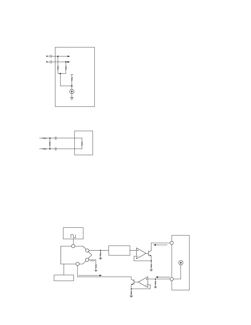
R = 2.5k , DATA
R = 3k , CLK
(TO FLIP-FLOPS)
400 A TYP
DATAP
DATAN
V
REG
R
50
50
Figure 7. AC Coupling of Data Inputs
For input signals that exceed 500 mV p-p single ended, it is
necessary to insert an attenuation circuit as shown in Figure 8.
R1
R2
R3
DATAP/CLKP
DATAN/CLKN
R
IN
ADN2847
NOTE THAT R
IN
= 100 = THE DIFFERENTIAL
INPUT IMPEDANCE OF THE ADN2847
Figure 8. Attenuation Circuit
CCBIAS
When the laser is used in ac-coupled mode, the CCBIAS and
I
BIAS
pins should be tied together (Figure 12). In dc-coupled
mode, CCBIAS should be tied to V
CC
.
Automatic Laser Shutdown
The ADN2847 ALS allows compliance to ITU-T-G958 (11/94),
section 9.7. When ALS is logic high, both bias and modulation
currents are turned off. Correct operation of ALS can be
confirmed by the FAIL alarm being raised when ALS is as-
serted. Note that this is the only time DEGRADE will be low
while FAIL is high.
Alarm Interfaces
The FAIL and DEGRADE outputs have an internal pull-up
resistor of 30 k
used to pull the digital high value to V
CC
.
However, the alarm can be overdriven with an external resistor
allowing alarm interfacing to non-V
CC
levels.
Non-V
CC
alarm
output levels must be below the V
CC
used for the ADN2847.
Power Consumption
The ADN2847 die temperature must be kept below 125
o
C. Both
LFCSP packages have an exposed paddle, which should be
connected in such a manner that is is at the same potential as
the ADN2847 ground pins. The
θ
JA
for both packages is shown
in the Absolute Maximum Ratings. Power consumption can be
calculated using
I
P
T
Thus, the maximum combination of
I
BIAS
+ I
MOD
must be calcu-
lated. Where:
I
CCMIN
=
50 mA, the typical value of I
CC
provided on page 3
with I
BIAS
= I
MOD
= 0
T
DIE
=
die temperature
T
AMBIENT
=
ambient temperature
V
BIAS_PIN
=
voltage at I
BIAS
pin
V
MODP_PIN
=
average voltage at IMODP pin
V
MODN_PIN
= average voltage at IMODN pin
Laser Diode Interfacing
Many laser diodes designed for 2.5 Gbs operation are packaged
with an internal resistor to bring the effective impedance up to
25
in order to minimize transmission line effects. In high current
applications, the voltage drop across this resistor combined with
the laser diode forward voltage makes direct connection between
the laser and the driver impractical in a 3 V system. AC coupling
the driver to the laser diode removes this headroom constraint.
I
I
×
CC
=
CCMIN
I
×
MOD
V
=
+ 0.3
+
V
I
I
V
V
CC
CC
BIAS
BIAS PIN
×
MOD
MODP
PIN
MODN
PIN
(
)
+
(
)
_
_
_
/
+
2
T
P
DIE
AMBIENT
A
=
+
θ
J
AD9850/AD9851
AD9834
DDS
50
I
OUT
1.25mA–20mA
21
I
OUT
50
R
SET
CONTROLLER
37.5 A–600 A
LP FILTER
(DC-COUPLED)
500
BC550
0.125mA–2mA
10kHz–1MHz
IDTONE
ADN2847
35
32
IMMON
50 A–800 A
1000
1/2
AD8602
BC550
1300
1/2
AD8602
CLKIN
REF CLOCK
20MHz–180MHz
9
20
12
Figure 9. Application Curcuit to Allow Fiber Identification Using the AD9850/AD9851
相關PDF資料 |
PDF描述 |
|---|---|
| ADN2847ACP-32 | 3 V Dual-Loop 50 Mbps to 3.3 Gbps Laser Diode Driver |
| ADN2847ACP-32-RL | 3 V Dual-Loop 50 Mbps to 3.3 Gbps Laser Diode Driver |
| ADN2847ACP-32-RL7 | 3 V Dual-Loop 50 Mbps to 3.3 Gbps Laser Diode Driver |
| ADN2847ACP-48 | 3 V Dual-Loop 50 Mbps to 3.3 Gbps Laser Diode Driver |
| ADN2847ACP-48-RL | 3 V Dual-Loop 50 Mbps to 3.3 Gbps Laser Diode Driver |
相關代理商/技術參數 |
參數描述 |
|---|---|
| ADN2847ACP-32 | 制造商:Analog Devices 功能描述:Laser Driver DFB 3.3Gbps 1-CH 32-Pin LFCSP EP |
| ADN2847ACP-32-RL | 制造商:Analog Devices 功能描述:Laser Driver DFB 3.3Gbps 1-CH 32-Pin LFCSP EP T/R |
| ADN2847ACP-32-RL7 | 制造商:Analog Devices 功能描述:Laser Driver DFB 3.3Gbps 1-CH 32-Pin LFCSP EP T/R |
| ADN2847ACP-48 | 制造商:Analog Devices 功能描述:Laser Driver DFB 3.3Gbps 1-CH 48-Pin LFCSP EP |
| ADN2847ACP-48-RL | 制造商:Analog Devices 功能描述:Laser Driver DFB 3.3Gbps 1-CH 48-Pin LFCSP EP T/R |
發布緊急采購,3分鐘左右您將得到回復。