- 您現在的位置:買賣IC網 > PDF目錄374019 > ADP1173AR-33 (Analog Devices, Inc.) RECTIFIER SCHOTTKY DUAL 40A 60V 375A-ifsm 0.7V-vf 1mA-ir TO-3P 30/TUBE PDF資料下載
參數資料
| 型號: | ADP1173AR-33 |
| 廠商: | Analog Devices, Inc. |
| 英文描述: | RECTIFIER SCHOTTKY DUAL 40A 60V 375A-ifsm 0.7V-vf 1mA-ir TO-3P 30/TUBE |
| 中文描述: | 微功率DC - DC轉換 |
| 文件頁數: | 9/16頁 |
| 文件大小: | 478K |
| 代理商: | ADP1173AR-33 |
ADP1173
–9–
REV. 0
+
I
LIM
V
IN
SW1
ADP1173
V
IN
L1
D1
C1
R2
R1
V
OUT
R3*
FB
* = OPTIONAL
SW2
GND
4
5
1
2
3
8
Figure 14. Step-Up Mode Operation
When the switch turns off, the magnetic field collapses. The
polarity across the inductor changes, current begins to flow
through D1 into the load and the output voltage is driven above
the input voltage.
The output voltage is fed back to the ADP1173 via resistors R1
and R2. When the voltage at pin FB falls below 1.245 V, SW1
turns “on” again and the cycle repeats. The output voltage is
therefore set by the formula:
V
OUT
=
1.245
V
×
1
+
R
1
R
2
The circuit of Figure 14 shows a direct current path from V
IN
to
V
OUT
, via the inductor and D1. Therefore, the boost converter
is not protected if the output is short circuited to ground.
CIRCUIT OPERATION, STEP-DOWN (BUCK) MODE
The ADP1173’s step-down mode is used to produce an output
voltage lower than the input voltage. For example, the output of
four NiCd cells (+4.8 V) can be converted to a +3.3 V logic
supply.
A typical configuration for step-down operation of the ADP1173
is shown in Figure 15. In this case, the collector of the internal
power switch is connected to V
IN
and the emitter drives the
inductor. When the switch turns on, SW2 is pulled up toward
V
IN
. This forces a voltage across L1 equal to (V
IN
–V
CE
) – V
OUT
,
and causes current to flow in L1. This current reaches a final
value of:
I
PEAK
V
IN
–
V
CE
–
V
OUT
L
×
23
μ
s
where 23
μ
s is the ADP1173 switch’s “on” time.
I
LIM
V
IN
FB
ADP1173
SW2
GND
5
1
2
8
SW1
3
R3
100
+
C2
V
IN
L1
D1
1N5818
+
C1
V
OUT
R2
R1
4
Figure 15. Step-Down Mode Operation
When the switch turns off, the magnetic field collapses. The
polarity across the inductor changes and the switch side of the
inductor is driven below ground. Schottky diode D1 then turns
on and current flows into the load. Notice that the Absolute
Maximum Rating for the ADP1173’s SW2 pin is 0.5 V below
ground. To avoid exceeding this limit, D1 must be a Schottky
diode. Using a silicon diode in this application will generate
forward voltages above 0.5 V, which will cause potentially
damaging power dissipation within the ADP1173.
The output voltage of the buck regulator is fed back to the
ADP1173’s FB pin by resistors R1 and R2. When the voltage at
pin FB falls below 1.245 V, the internal power switch turns
“on” again and the cycle repeats. The output voltage is set by
the formula:
V
OUT
=
1.245
V
×
1
+
R
1
R
2
When operating the ADP1173 in step-down mode, the output
voltage is impressed across the internal power switch’s emitter-
base junction when the switch is off. To protect the switch, the
output voltage should be limited to 6.2 V or less. If a higher
output voltage is required, a Schottky diode should be placed in
series with SW2, as shown in Figure 16.
If high output current is required in a step-down converter, the
ADP1111 or ADP3000 should be considered. These devices
offer higher frequency operation, which reduces inductor size,
and an external pass transistor can be added to reduce R
ON
of
the switch.
I
LIM
V
IN
FB
ADP1173
SW2
GND
5
1
2
8
SW1
3
R
LIM
100
+
C2
L1
D1
1N5818
+
C1
V
OUT
R2
R1
1N5818
V
IN
4
Figure 16. Step-Down Mode, V
OUT
> 6.2 V
If the input voltage to the ADP1173 varies over a wide range, a
current limiting resistor at Pin 1 may be required. If a particular
circuit requires high peak inductor current with minimum input
supply voltage, the peak current may exceed the switch maxi-
mum rating and/or saturate the inductor when the supply
voltage is at the maximum value. See the Limiting the Switch
Current section of this data sheet for specific recommendations.
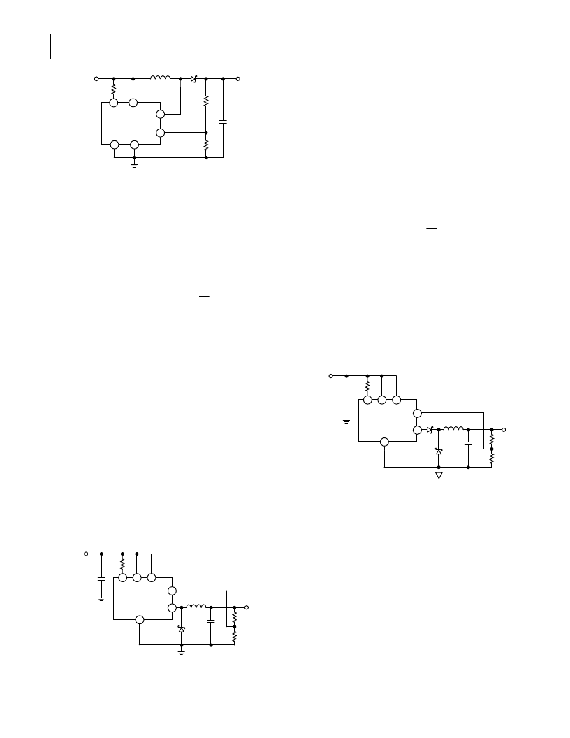
POSITIVE-TO-NEGATIVE CONVERSION
The ADP1173 can convert a positive input voltage to a negative
output voltage, as shown in Figure 17. This circuit is essentially
identical to the step-down application of Figure 15, except that
the “output” side of the inductor is connected to power ground.
When the ADP1173’s internal power switch turns off, current
flowing in the inductor forces the output (–V
OUT
) to a negative
potential. The ADP1173 will continue to turn the switch on
相關PDF資料 |
PDF描述 |
|---|---|
| ADP1173AR-5 | RECTIFIER SCHOTTKY SINGLE 5A 40V 175A-ifsm 0.55V-vf 0.5mA-ir TO220AC 50/TUBE |
| ADP1610 | 1.2 MHz DC-DC Step-Up Switching Converter |
| ADP1610ARMZ-R7 | 1.2 MHz DC-DC Step-Up Switching Converter |
| ADP3000AR-33 | Circular Connector Cable Assembly; Connector Type A:Circular Plug; Connector Type B:Stripped End Leads; Cable Length:10ft RoHS Compliant: Yes |
| ADP3000 | Isolated Flyback Switching Regulator with 9V Output |
相關代理商/技術參數 |
參數描述 |
|---|---|
| ADP1173AR-5 | 制造商:Rochester Electronics LLC 功能描述:MICROPOWER DC-DC CONVERTER 5V - Bulk |
| ADP1181 | 功能描述:板上安裝壓力/力傳感器 833.6kPa 8.5kgf/cm Pressure Sensor RoHS:否 制造商:Honeywell 工作壓力:0 bar to 4 bar 壓力類型:Gage 準確性:+ / - 0.25 % 輸出類型:Digital 安裝風格:Through Hole 工作電源電壓:5 V 封裝 / 箱體:SIP 端口類型:Dual Radial Barbed, Same sides |
| ADP1190 | 制造商:AD 制造商全稱:Analog Devices 功能描述:Integrated 500 mA Load Switch with Quad Signal Switch |
| ADP1190AACBZ-R7 | 制造商:Analog Devices 功能描述:LOAD SWITCH QUAD SIGNAL SWITCH EN LOW - Tape and Reel 制造商:Analog Devices 功能描述:IC HIGH-SIDE LOAD SWITCH 12WLCSP 制造商:Analog Devices 功能描述:IC LOW-SIDE LOAD SWITCH 12WLCSP 制造商:Analog Devices 功能描述:LOAD SWITCH, HIGH SIDE, 3.6V, WLCSP-12, Power Load Switch Type:High Side, Input Voltage:3.6V, Current Limit:500mA, On State Resistance:0.065ohm, Distribution Switch Case Style:WLCSP, No. of Pins:12, Thermal Protection:Yes |
| ADP1190ACBZ-R7 | 功能描述:電源開關 IC - 配電 RoHS:否 制造商:Exar 輸出端數量:1 開啟電阻(最大值):85 mOhms 開啟時間(最大值):400 us 關閉時間(最大值):20 us 工作電源電壓:3.2 V to 6.5 V 電源電流(最大值): 最大工作溫度:+ 85 C 安裝風格:SMD/SMT 封裝 / 箱體:SOT-23-5 |
發布緊急采購,3分鐘左右您將得到回復。