- 您現(xiàn)在的位置:買賣IC網(wǎng) > PDF目錄374019 > ADP3156JR-18 (Analog Devices, Inc.) Dual Power Supply Controller for Desktop Systems PDF資料下載
參數(shù)資料
| 型號: | ADP3156JR-18 |
| 廠商: | Analog Devices, Inc. |
| 英文描述: | Dual Power Supply Controller for Desktop Systems |
| 中文描述: | 雙電源控制器桌面系統(tǒng) |
| 文件頁數(shù): | 10/12頁 |
| 文件大小: | 186K |
| 代理商: | ADP3156JR-18 |
REV. 0
ADP3156
–10–
Feedback Loop Compensation Design for Active Voltage
Positioning
Optimized compensation of the ADP3156 allows the best pos-
sible containment of the peak-to-peak output voltage deviation.
Any practical switching power converter is inherently limited by
the inductor in its output current slew rate to a value much less
than the slew rate of the load. Therefore, any sudden change of
load current will initially flow through the output capacitors,
and this will produce an output voltage deviation equal to the
ESR of the output capacitor array times the load current change.
To correctly implement active voltage positioning, the low fre-
quency output impedance (i.e., the output resistance) of the
converter should be made equal to the maximum ESR of the
output capacitor array. This can be achieved by having a single
pole roll-off of the voltage gain of the g
m
error amplifier, where
the pole frequency coincides with the ESR zero of the output
capacitor. A gain with single pole roll-off requires that the g
m
amplifier output pin be terminated by the parallel combination
of a resistor and capacitor. The required resistor value can be
calculated from the equation:
R
k
k
Rt
Rt
C
TOTAL
TOTAL
=
×
275
275
–
where:
Rt
k
R
–
I
V
V
TOTAL
CS
OMAX
HI
LO
=
×
×
16 4
where the quantities 16.4 k
and 275 k
are characteristics of
the ADP3156, the value of the current sense resistor, R
CS
, has
already been determined as above, and where V
HI
and V
LO
are
the respective upper and lower limits allowed for regulation.
Although a single termination resistor equal to R
C
would yield
the proper voltage positioning gain, the dc biasing of that resis-
tor would determine how the regulation band is centered (i.e.,
note that sometimes the specified regulation band is asymmetri-
cal with respect to the nominal VID voltage.) With the ADP3156,
the offset is already considered as part of the design procedure—
no special provision is required. To accomplish the dc biasing, it
is simplest to use two resistors to terminate the g
m
output, with
the lower resistor tied to ground and the upper resistor to the
12 V supply of the IC. The values of these resistors can be cal-
culated using:
R
R
V
V
UPPER
C
DIV
OS
=
×
and:
R
R
V
V
V
LOWER
C
OS
–
DIV
OS
=
×
where
V
DIV
is the resistor divider supply voltage (e.g., the rec-
ommended 12 V), and V
OS
is the offset voltage required on the
amplifier to produce the desired offset at the output. V
OS
is
calculated using Equation 2, where V
OUT(OS)
is the offset from
the nominal VID-programmed value to the center of the speci-
fied regulation window for the output voltage. (Note this may be
either positive or negative.) For clarification, that offset is given
by:
V
V
(
V
VID
OUT OS
HI
LO
(
)
)
–
=
+
1
2
Finally, the compensating capacitance is determined from the
equality of the pole frequency of the error amplifier gain and the
zero frequency of the impedance of the output capacitor:
C
C
ESR
Rt
COMP
O
TOTAL
=
×
Trade-Offs Between DC Load Regulation and AC Load
Regulation
Casual observation of the circuit operation—e.g., with a volt-
meter—would make it appear that the dc load regulation ap-
pears to be rather poor compared to a conventional regulator.
This would be especially noticeable under very light or very
heavy loads where the voltage is “positioned” near one of the
extremes of the regulation window rather than near the nominal
center value. It must be noted and understood that this low gain
characteristic (i.e., loose dc load regulation) is inherently re-
quired to allow improved transient containment (i.e., to achieve
tighter ac load regulation). That is, the dc load regulation is
intentionally sacrificed (but kept within specification) in order
to minimize the number of capacitors required to contain the
load transients produced by the CPU.
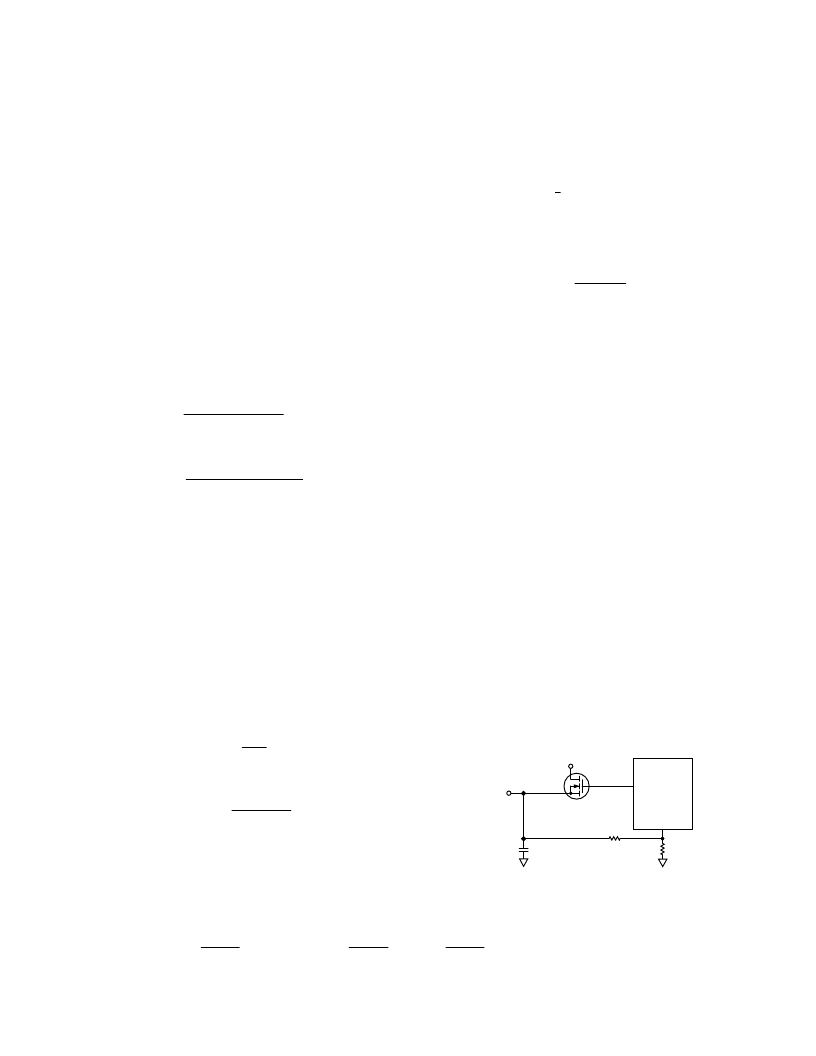
Linear Regulator
The ADP3156 linear regulator provides a low cost, convenient
and versatile solution for generating a lower supply rail in addi-
tion to the main output. The maximum output load current is
determined by the size and thermal impedance of the external
N-channel power MOSFET that is controlled by the ADP3156.
The output voltage, V
O2
in Figure 14, is sensed at the FB pin of
the ADP3156 and compared to an internal 1.2 V reference in a
negative feedback loop which keeps the output voltage in regula-
tion. If the load is being reduced or increased, the FET drive
will also be reduced or increased by the ADP3156 to provide a
well regulated
±
1% accurate output voltage. The output voltage
is programmed by adjusting the value of the external resistor
R
PROG
, shown in Figure 14.
V
IN
= +1.8V
IRL3103
1000
m
F/10V
V
LDO
ADP3156
FB
20k
V
V
O2
= +1.5V
I
O2
= 4.0A
R
PROG
5k
Figure 14. Linear Regulator Configuration
V
R
Rt
V
V
Rt
1 36
.
k
V
Rt
275
k
R I
OS
C
TOTAL
OUT OS
TOTAL
TOTAL
=
×
+
+
0 8
.
6
–1 7
(
)
(2)
相關(guān)PDF資料 |
PDF描述 |
|---|---|
| ADP3156JR-25 | Dual Power Supply Controller for Desktop Systems |
| ADP3156 | Dual Power Supply Controller for Desktop Systems |
| ADP3160 | 5-Bit Programmable 2-Phase Synchronous Buck Controller |
| ADP3160JR | 5-Bit Programmable 2-Phase Synchronous Buck Controller |
| ADP3167JR | 5-Bit Programmable 2-Phase Synchronous Buck Controller |
相關(guān)代理商/技術(shù)參數(shù) |
參數(shù)描述 |
|---|---|
| ADP3156JR-2.5 | 制造商:Rochester Electronics LLC 功能描述:- Bulk |
| ADP3156JR-25 | 制造商:AD 制造商全稱:Analog Devices 功能描述:Dual Power Supply Controller for Desktop Systems |
| ADP3157 | 制造商:AD 制造商全稱:Analog Devices 功能描述:5-Bit Programmable Synchronous Controller for Pentium III Processors |
| ADP3157J | 制造商:Analog Devices 功能描述: |
| ADP3157JR | 制造商:Rochester Electronics LLC 功能描述:- Bulk |
發(fā)布緊急采購,3分鐘左右您將得到回復(fù)。