- 您現在的位置:買賣IC網 > PDF目錄374019 > ADP3156JR-18 (Analog Devices, Inc.) Dual Power Supply Controller for Desktop Systems PDF資料下載
參數資料
| 型號: | ADP3156JR-18 |
| 廠商: | Analog Devices, Inc. |
| 英文描述: | Dual Power Supply Controller for Desktop Systems |
| 中文描述: | 雙電源控制器桌面系統 |
| 文件頁數: | 12/12頁 |
| 文件大小: | 186K |
| 代理商: | ADP3156JR-18 |
REV. 0
ADP3156
–12–
C
P
9. Absolutely avoid crossing any signal lines over the switching
power path loop, described below.
Power Circuitry
10. The switching power path should be routed on the PCB to
encompass the smallest possible area in order to minimize
radiated switching noise energy (i.e., EMI). Failure to take
proper precaution often results in EMI problems for the
entire PC system as well as noise-related operational prob-
lems in the power converter control circuitry. The switching
power path is the loop formed by the current path through
the input capacitors, the two FETs, and the power Schottky
diode if used, including all interconnecting PCB traces and
planes. The use of short and wide interconnection traces is
especially critical in this path for two reasons: it minimizes
the inductance in the switching loop, which can cause high-
energy ringing, and it accommodates the high current de-
mand with minimal voltage loss.
11. A power Schottky diode (1~2 Adc rating) placed from the
lower FET’s source (anode) to drain (cathode) will help to
minimize switching power dissipation in the upper FET. In
the absence of an effective Schottky diode, this dissipation
occurs through the following sequence of switching events.
The lower FET turns off in advance of the upper FET turn-
ing on (necessary to prevent cross-conduction). The circu-
lating current in the power converter, no longer finding a
path for current through the channel of the lower FET,
draws current through the inherent body-drain diode of the
FET. The upper FET turns on, and the reverse recovery
characteristic of the lower FET’s body-drain diode prevents
the drain voltage from being pulled high quickly. The upper
FET then conducts very large current while it momentarily
has a high voltage forced across it, which translates into
added power dissipation in the upper FET. The Schottky
diode minimizes this problem by carrying a majority of the
circulating current when the lower FET is turned off, and by
virtue of its essentially nonexistent reverse recovery time.
12. A small ferrite bead inductor placed in series with the drain
of the lower FET can also help to reduce this previously
described source of switching power loss.
13. Whenever a power dissipating component (e.g., a power
MOSFET) is soldered to a PCB, the liberal use of vias both
directly on the mounting pad and immediately surrounding
it is recommended. Two important reasons for this are:
improved current rating through the vias (if it is a current
path), and improved thermal performance—especially if the
vias extended to the opposite side of the PCB where a plane
can more readily transfer the heat to the air.
14. The output power path, though not as critical as the switch-
ing power path, should also be routed to encompass a small
area. The output power path is formed by the current path
through the inductor, the current sensing resistor, the out-
put capacitors, and back to the input capacitors.
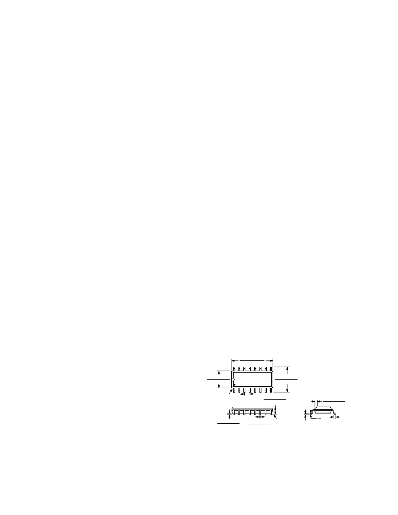
OUTLINE DIMENSIONS
Dimensions shown in inches and (mm).
16-Lead Standard Small Outline Package (SOIC)
(R-16A)
16
9
8
1
0.2440 (6.20)
0.2284 (5.80)
0.1574 (4.00)
0.1497 (3.80)
PIN 1
0.3937 (10.00)
0.3859 (9.80)
0.050 (1.27)
BSC
SEATING
PLANE
0.0098 (0.25)
0.0040 (0.10)
0.0192 (0.49)
0.0138 (0.35)
0.0688 (1.75)
0.0532 (1.35)
8
8
0
8
0.0196 (0.50)
0.0099 (0.25)
3
45
8
0.0500 (1.27)
0.0160 (0.41)
0.0099 (0.25)
0.0075 (0.19)
15. For best EMI containment, the power ground plane should
extend fully under all the power components except the
output capacitors. These are: the input capacitors, the power
MOSFETs and Schottky diode, the inductor, the current
sense resistor, and any snubbing elements that might be
added to dampen ringing. Avoid extending the power ground
under any other circuitry or signal lines, including the volt-
age and current sense lines.
Signal Circuitry
16. The output voltage is sensed and regulated between the
AGND pin (which connects to the signal ground plane) and
the SENSE– pin. The output current is sensed (as a voltage)
and regulated between the SENSE– pin and the SENSE+
pin. In order to avoid differential mode noise pickup in
those sensed signals, their loop areas should be small. Thus
the SENSE– trace should be routed atop the signal ground
plane, and the SENSE+ and SENSE– traces should be routed
as a closely coupled pair (SENSE+ should be over the signal
ground plane as well).
17. The SENSE+ and SENSE– traces should be Kelvin con-
nected to the current sense resistor so that the additional
voltage drop due to current flow on the PCB at the current
sense resistor connections does not affect the sensed voltage.
It is desirable to both have the ADP3156 close to the output
capacitor bank and not in the output power path so that any
voltage drop between the output capacitors and the AGND
pin is minimized, and voltage regulation is not compromised.
相關PDF資料 |
PDF描述 |
|---|---|
| ADP3156JR-25 | Dual Power Supply Controller for Desktop Systems |
| ADP3156 | Dual Power Supply Controller for Desktop Systems |
| ADP3160 | 5-Bit Programmable 2-Phase Synchronous Buck Controller |
| ADP3160JR | 5-Bit Programmable 2-Phase Synchronous Buck Controller |
| ADP3167JR | 5-Bit Programmable 2-Phase Synchronous Buck Controller |
相關代理商/技術參數 |
參數描述 |
|---|---|
| ADP3156JR-2.5 | 制造商:Rochester Electronics LLC 功能描述:- Bulk |
| ADP3156JR-25 | 制造商:AD 制造商全稱:Analog Devices 功能描述:Dual Power Supply Controller for Desktop Systems |
| ADP3157 | 制造商:AD 制造商全稱:Analog Devices 功能描述:5-Bit Programmable Synchronous Controller for Pentium III Processors |
| ADP3157J | 制造商:Analog Devices 功能描述: |
| ADP3157JR | 制造商:Rochester Electronics LLC 功能描述:- Bulk |
發布緊急采購,3分鐘左右您將得到回復。