- 您現在的位置:買賣IC網 > PDF目錄374032 > ADSP-21060L (Analog Devices, Inc.) ADSP-2106x SHARC DSP Microcomputer Family PDF資料下載
參數資料
| 型號: | ADSP-21060L |
| 廠商: | Analog Devices, Inc. |
| 英文描述: | ADSP-2106x SHARC DSP Microcomputer Family |
| 中文描述: | 的ADSP - 2106x SHARC處理器DSP的微機家庭 |
| 文件頁數: | 3/47頁 |
| 文件大小: | 366K |
| 代理商: | ADSP-21060L |
第1頁第2頁當前第3頁第4頁第5頁第6頁第7頁第8頁第9頁第10頁第11頁第12頁第13頁第14頁第15頁第16頁第17頁第18頁第19頁第20頁第21頁第22頁第23頁第24頁第25頁第26頁第27頁第28頁第29頁第30頁第31頁第32頁第33頁第34頁第35頁第36頁第37頁第38頁第39頁第40頁第41頁第42頁第43頁第44頁第45頁第46頁第47頁
ADSP-21060/ADSP-21060L
–3–
REV. D
GENERAL DESCRIPTION
The ADSP-21060 SHARC—Super Harvard Architecture Com-
puter—is a signal processing microcomputer that offers new
capabilities and levels of performance. The ADSP-2106x
SHARCs are 32-bit processors optimized for high performance
DSP applications. The ADSP-2106x builds on the ADSP-
21000 DSP core to form a complete system-on-a-chip, adding a
dual-ported on-chip SRAM and integrated I/O peripherals sup-
ported by a dedicated I/O bus.
Fabricated in a high speed, low power CMOS process, the
ADSP-2106x has a 25 ns instruction cycle time and operates
at 40 MIPS. With its on-chip instruction cache, the processor
can execute every instruction in a single cycle. Table I shows
performance benchmarks for the ADSP-2106x.
The ADSP-2106x SHARC represents a new standard of inte-
gration for signal computers, combining a high performance
floating-point DSP core with integrated, on-chip system features
including a 4 Mbit SRAM memory host processor interface,
DMA controller, serial ports, and link port and parallel bus
connectivity for glueless DSP multiprocessing.
Figure 1 shows a block diagram of the ADSP-2106x, illustrating
the following architectural features:
Computation Units (ALU, Multiplier and Shifter) with a
Shared Data Register File
Data Address Generators (DAG1, DAG2)
Program Sequencer with Instruction Cache
Interval Timer
On-Chip SRAM
External Port for Interfacing to Off-Chip Memory and
Peripherals
Host Port and Multiprocessor Interface
DMA Controller
Serial Ports and Link Ports
JTAG Test Access Port
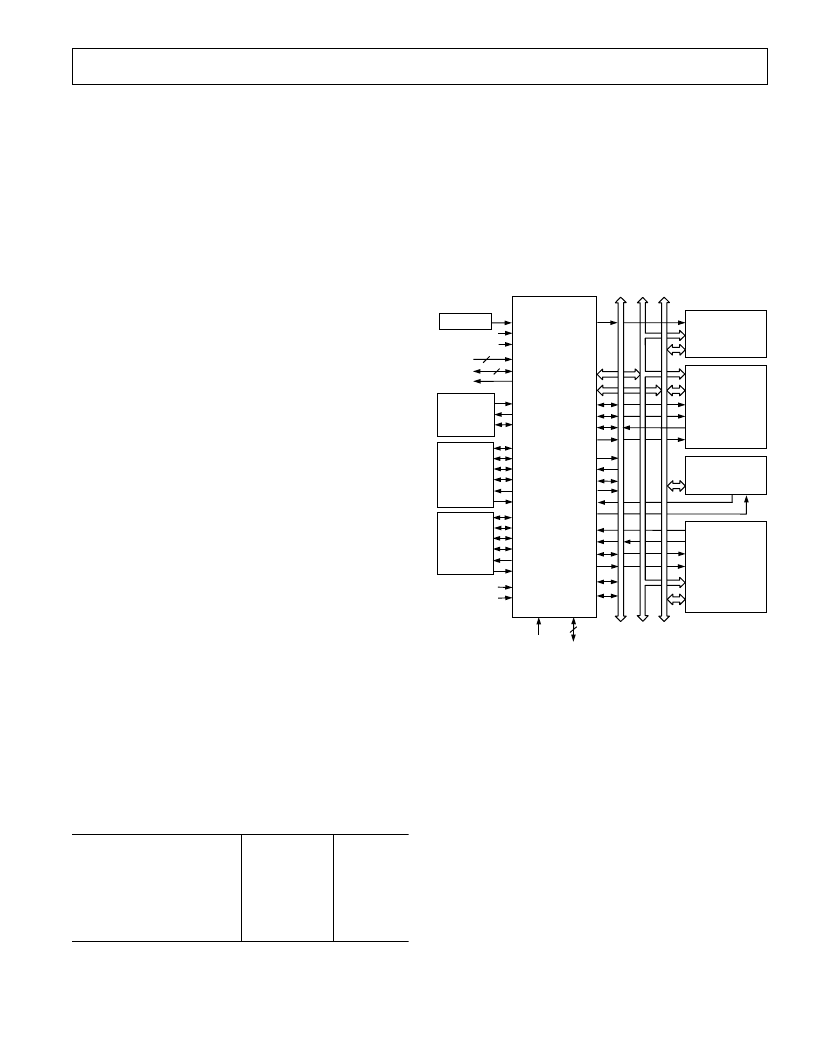
Figure 2 shows a typical single-processor system. A multi-
processing system is shown in Figure 3.
Table I. ADSP-21060/ADSP-21060L Benchmarks (@ 40 MHz)
1024-Pt. Complex FFT
(Radix 4, with Digit Reverse)
FIR Filter (per Tap)
IIR Filter (per Biquad)
Divide (y/x)
Inverse Square Root (1/
√
x
)
DMA Transfer Rate
0.46 ms
18,221 cycles
25 ns
100 ns
150 ns
225 ns
240 Mbytes/s
1 cycle
4 cycles
6 cycles
9 cycles
ADSP-21000 FAMILY CORE ARCHITECTURE
The ADSP-2106x includes the following architectural features
of the ADSP-21000 family core. The ADSP-21060 is code- and
function-compatible with the ADSP-21061 and ADSP-21062.
Independent, Parallel Computation Units
The arithmetic/logic unit (ALU), multiplier and shifter all per-
form single-cycle instructions. The three units are arranged in
parallel, maximizing computational throughput. Single multi-
function instructions execute parallel ALU and multiplier opera-
tions. These computation units support IEEE 32-bit single-
precision floating-point, extended precision 40-bit floating-
point, and 32-bit fixed-point data formats.
3
4
RESET
JTAG
7
ADSP-2106x
BMS
ADDR
31-0
DATA
47-0
C
A
D
CS
ADDR
DATA
BOOT
EPROM
(OPTIONAL)
ADDR
ACK
CS
MEMORY
AND
PERIPHERALS
(OPTIONAL)
OE
WE
DATA
DMA DEVICE
(OPTIONAL)
DATA
ADDR
DATA
HOST
PROCESSOR
INTERFACE
(OPTIONAL)
1x CLOCK
LINK
DEVICES
(6 MAXIMUM)
(OPTIONAL)
SERIAL
DEVICE
(OPTIONAL)
CS
HBR
HBG
REDY
RD
WR
ACK
MS
3-0
PAGE
SBTS
SW
ADRCLK
DMAR1-2
DMAG1-2
BR
1-6
CPA
SERIAL
DEVICE
(OPTIONAL)
CLKIN
EBOOT
LBOOT
IRQ
2-0
FLAG
3-0
TIMEXP
LxCLK
LxACK
LxDAT
3-0
TCLK0
RCLK0
TFS0
RSF0
DT0
DR0
TCLK1
RCLK1
TFS1
RFS1
DT1
DR1
RPBA
ID
2-0
Figure 2. ADSP-2106x System
Data Register File
A general purpose data register file is used for transferring data
between the computation units and the data buses, and for
storing intermediate results. This 10-port, 32-register (16 pri-
mary, 16 secondary) register file, combined with the ADSP-
21000 Harvard architecture, allows unconstrained data flow
between computation units and internal memory.
Single-Cycle Fetch of Instruction and Two Operands
The ADSP-2106x features an enhanced Harvard architecture in
which the data memory (DM) bus transfers data and the pro-
gram memory (PM) bus transfers both instructions and data
(see Figure 1). With its separate program and data memory
buses and on-chip instruction cache, the processor can simulta-
neously fetch two operands and an instruction (from the cache),
all in a single cycle.
S
相關PDF資料 |
PDF描述 |
|---|---|
| ADSP-21060LAB-160 | ADSP-2106x SHARC DSP Microcomputer Family |
| ADSP-21060KS-133 | ADSP-2106x SHARC DSP Microcomputer Family |
| ADSP-21060KS-160 | ADSP-2106x SHARC DSP Microcomputer Family |
| ADSP-21060LKB-160 | RES, 2.2 K SM CHIP 5% 50V 1/16 WATT, 0603 |
| ADSP-21060LKS-133 | ADSP-2106x SHARC DSP Microcomputer Family |
相關代理商/技術參數 |
參數描述 |
|---|---|
| ADSP-21060LAB-160 | 功能描述:IC DSP CONTROLLER 32BIT 225BGA RoHS:否 類別:集成電路 (IC) >> 嵌入式 - DSP(數字式信號處理器) 系列:SHARC® 標準包裝:2 系列:StarCore 類型:SC140 內核 接口:DSI,以太網,RS-232 時鐘速率:400MHz 非易失內存:外部 芯片上RAM:1.436MB 電壓 - 輸入/輸出:3.30V 電壓 - 核心:1.20V 工作溫度:-40°C ~ 105°C 安裝類型:表面貼裝 封裝/外殼:431-BFBGA,FCBGA 供應商設備封裝:431-FCPBGA(20x20) 包裝:托盤 |
| ADSP-21060LABZ-160 | 功能描述:IC DSP CONTROLLER 32BIT 225-BGA RoHS:是 類別:集成電路 (IC) >> 嵌入式 - DSP(數字式信號處理器) 系列:SHARC® 標準包裝:2 系列:StarCore 類型:SC140 內核 接口:DSI,以太網,RS-232 時鐘速率:400MHz 非易失內存:外部 芯片上RAM:1.436MB 電壓 - 輸入/輸出:3.30V 電壓 - 核心:1.20V 工作溫度:-40°C ~ 105°C 安裝類型:表面貼裝 封裝/外殼:431-BFBGA,FCBGA 供應商設備封裝:431-FCPBGA(20x20) 包裝:托盤 |
| ADSP-21060LC | 制造商:未知廠家 制造商全稱:未知廠家 功能描述:ADSP-21060C/ADSP-21060LC: Industrial Sharc?DSP Microcomputer Family Data Sheet (Rev. B. 10/00) |
| ADSP-21060LCB-133 | 功能描述:IC DSP CONTROLLER 32BIT 225BGA RoHS:否 類別:集成電路 (IC) >> 嵌入式 - DSP(數字式信號處理器) 系列:SHARC® 標準包裝:2 系列:StarCore 類型:SC140 內核 接口:DSI,以太網,RS-232 時鐘速率:400MHz 非易失內存:外部 芯片上RAM:1.436MB 電壓 - 輸入/輸出:3.30V 電壓 - 核心:1.20V 工作溫度:-40°C ~ 105°C 安裝類型:表面貼裝 封裝/外殼:431-BFBGA,FCBGA 供應商設備封裝:431-FCPBGA(20x20) 包裝:托盤 |
| ADSP-21060LCBZ-133 | 功能描述:IC DSP CONTROLLER 32BIT 225PBGA RoHS:是 類別:集成電路 (IC) >> 嵌入式 - DSP(數字式信號處理器) 系列:SHARC® 標準包裝:2 系列:StarCore 類型:SC140 內核 接口:DSI,以太網,RS-232 時鐘速率:400MHz 非易失內存:外部 芯片上RAM:1.436MB 電壓 - 輸入/輸出:3.30V 電壓 - 核心:1.20V 工作溫度:-40°C ~ 105°C 安裝類型:表面貼裝 封裝/外殼:431-BFBGA,FCBGA 供應商設備封裝:431-FCPBGA(20x20) 包裝:托盤 |
發布緊急采購,3分鐘左右您將得到回復。