- 您現(xiàn)在的位置:買賣IC網(wǎng) > PDF目錄374033 > ADSP-21262SKSTZ200 (ANALOG DEVICES INC) SHARC Processor PDF資料下載
參數(shù)資料
| 型號: | ADSP-21262SKSTZ200 |
| 廠商: | ANALOG DEVICES INC |
| 元件分類: | 數(shù)字信號處理 |
| 英文描述: | SHARC Processor |
| 中文描述: | 16-BIT, 66.67 MHz, OTHER DSP, PQFP144 |
| 封裝: | LEAD FREE, MS-026BFB, LQFP-144 |
| 文件頁數(shù): | 37/44頁 |
| 文件大小: | 1295K |
| 代理商: | ADSP-21262SKSTZ200 |
第1頁第2頁第3頁第4頁第5頁第6頁第7頁第8頁第9頁第10頁第11頁第12頁第13頁第14頁第15頁第16頁第17頁第18頁第19頁第20頁第21頁第22頁第23頁第24頁第25頁第26頁第27頁第28頁第29頁第30頁第31頁第32頁第33頁第34頁第35頁第36頁當前第37頁第38頁第39頁第40頁第41頁第42頁第43頁第44頁
ADSP-21262
Rev. A
|
Page 37 of 44
|
May 2004
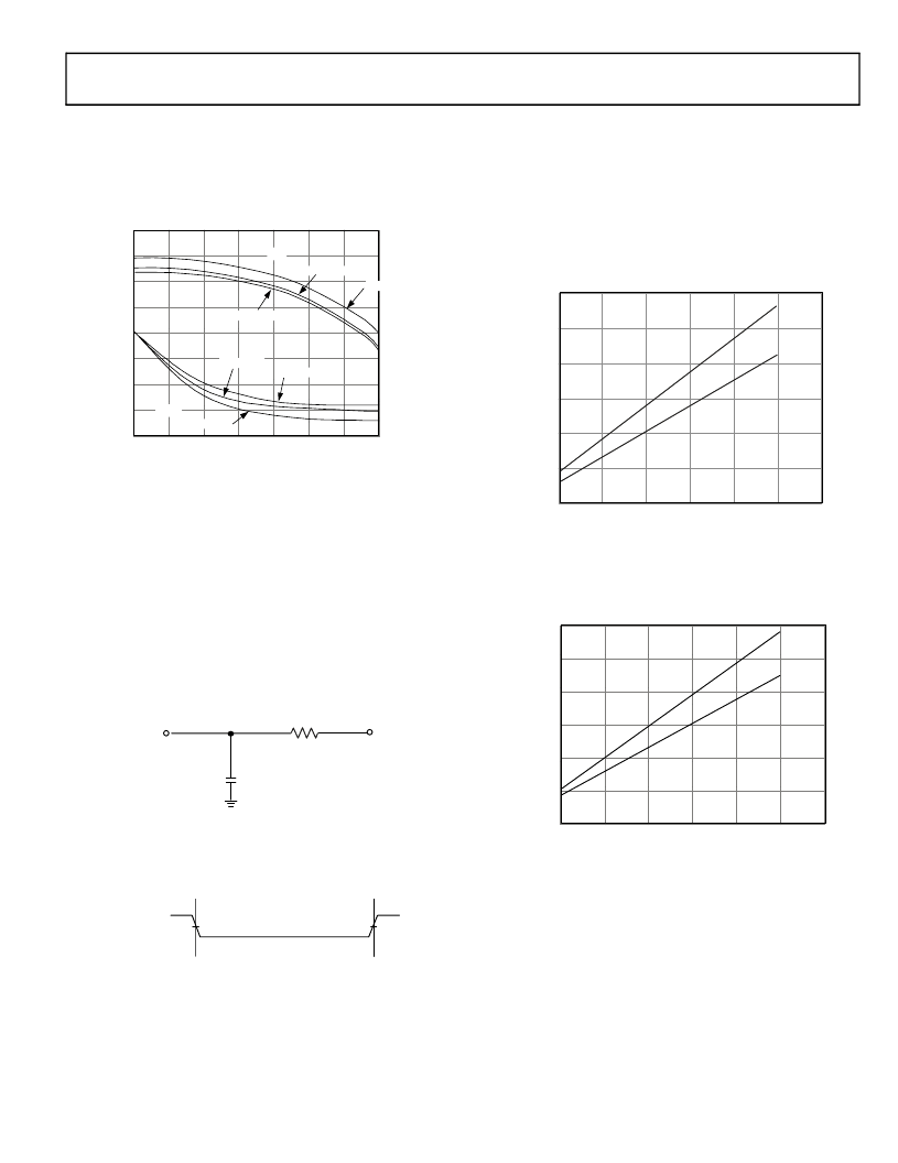
OUTPUT DRIVE CURRENTS
Figure 28
shows typical I-V characteristics for the output driv-
ers of the ADSP-21262. The curves represent the current drive
capability of the output drivers as a function of output voltage.
TEST CONDITIONS
The ac signal specifications (timing parameters) appear in
Table 10 on Page 19
through
Table 31 on Page 36
. These include
output disable time, output enable time, and capacitive loading.
Timing is measured on signals when they cross the 1.5 V level as
described in
Figure 30
. All delays (in nanoseconds) are mea-
sured between the point that the first signal reaches 1.5 V and
the point that the second signal reaches 1.5 V.
CAPACITIVE LOADING
Output delays and holds are based on standard capacitive loads:
30 pF on all pins (see
Figure 29
).
Figure 33
shows graphically
how output delays and holds vary with load capacitance. The
graphs of
Figure 31
,
Figure 32
, and
Figure 33
may not be linear
outside the ranges shown for Typical Output Delay vs. Load
Capacitance and Typical Output Rise Time (20% – 80%, V =
Min) vs. Load Capacitance.
Figure 28. ADSP-21262 Typical Drive
Figure 29. Equivalent Device Loading for AC Measurements
(Includes All Fixtures)
Figure 30. Voltage Reference Levels for AC Measurements
SWEEP (VDDEXT) VOLTAGE (V)
-20
0
3.5
0.5
1
1.5
2
2.5
3
0
-40
-30
20
40
-10
S
VOL
3.11V, 70° C
3.3V, 25° C
3.47V, 0° C
VOH
30
10
3.11V, 70° C
3.3V, 25° C
3.47V, 0° C
1.5V
30pF
TO
OUTPUT
PIN
50
INPUT
OR
OUTPUT
1.5V
1.5V
Figure 31. Typical Output Rise/Fall Time
(20%-80%, V
DDEXT
= Max)
Figure 32. Typical Output Rise/Fall Time
(20%-80%, V
DDEXT
= Min)
LOAD CAPACITANCE (pF)
8.0
0
0
120
40
100
12.0
4.0
2.0
10.0
6.0
R
y = 0.0904x + 1.9426
y = 0.0722x + 1.4042
80
60
20
RISE
FALL
LOAD CAPACITANCE (pF)
12
0
120
20
40
60
80
100
10
8
6
4
R
2
0
y = 0.0915x + 2.2207
y = 0.0728x +1.6336
RISE
FALL
相關PDF資料 |
PDF描述 |
|---|---|
| ADSP-21262 | SHARC Processor |
| ADSP-21262SKBC-200 | SHARC Processor |
| ADSP-21262SKBCZ200 | SHARC Processor |
| ADSP-21266 | SHARC Embedded Processor |
| ADSP-21266SKBC-2B | SHARC Embedded Processor |
相關代理商/技術參數(shù) |
參數(shù)描述 |
|---|---|
| ADSP-21262SKSTZ200 | 制造商:Analog Devices 功能描述:IC 32-BIT DSP |
| ADSP-21266 | 制造商:AD 制造商全稱:Analog Devices 功能描述:SHARC Embedded Processor |
| ADSP-21266_07 | 制造商:AD 制造商全稱:Analog Devices 功能描述:Embedded Processor |
| ADSP-21266KSTZ-1C | 制造商:Analog Devices 功能描述:- Trays |
| ADSP-21266KSTZ-2C | 制造商:Analog Devices 功能描述:- Trays |
發(fā)布緊急采購,3分鐘左右您將得到回復。