- 您現在的位置:買賣IC網 > PDF目錄374039 > ADUC842BCP62-3 (ANALOG DEVICES INC) MicroConverter 12-Bit ADCs and DACs with Embedded High Speed 62-kB Flash MCU PDF資料下載
參數資料
| 型號: | ADUC842BCP62-3 |
| 廠商: | ANALOG DEVICES INC |
| 元件分類: | 微控制器/微處理器 |
| 英文描述: | MicroConverter 12-Bit ADCs and DACs with Embedded High Speed 62-kB Flash MCU |
| 中文描述: | 8-BIT, FLASH, 8.38 MHz, MICROCONTROLLER, QCC56 |
| 封裝: | 8 X 8 MM, LEAD FRAME, MO-220VLLD2, CSP-56 |
| 文件頁數: | 47/88頁 |
| 文件大小: | 903K |
| 代理商: | ADUC842BCP62-3 |
第1頁第2頁第3頁第4頁第5頁第6頁第7頁第8頁第9頁第10頁第11頁第12頁第13頁第14頁第15頁第16頁第17頁第18頁第19頁第20頁第21頁第22頁第23頁第24頁第25頁第26頁第27頁第28頁第29頁第30頁第31頁第32頁第33頁第34頁第35頁第36頁第37頁第38頁第39頁第40頁第41頁第42頁第43頁第44頁第45頁第46頁當前第47頁第48頁第49頁第50頁第51頁第52頁第53頁第54頁第55頁第56頁第57頁第58頁第59頁第60頁第61頁第62頁第63頁第64頁第65頁第66頁第67頁第68頁第69頁第70頁第71頁第72頁第73頁第74頁第75頁第76頁第77頁第78頁第79頁第80頁第81頁第82頁第83頁第84頁第85頁第86頁第87頁第88頁
ADuC841/ADuC842/ADuC843
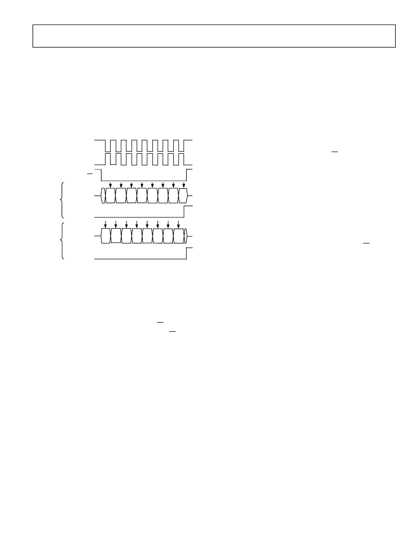
Using the SPI Interface
Depending on the configuration of the bits in the SPICON SFR
shown in Table 18, the ADuC841/ADuC842/ADuC843 SPI
interface transmits or receives data in a number of possible
modes. Figure 54 shows all possible SPI configurations for the
parts, and the timing relationships and synchronization
between the signals involved. Also shown in this figure is the
SPI interrupt bit (ISPI) and how it is triggered at the end of each
byte-wide communication.
Rev. 0 | Page 47 of 88
SCLOCK
(CPOL = 1)
SCLOCK
(CPOL = 0)
(CPHA = 1)
(CPHA = 0)
SAMPLE INPUT
ISPI FLAG
DATA OUTPUT
ISPI FLAG
SAMPLE INPUT
DATA OUTPUT
MSB BIT 6 BIT 5
BIT 4 BIT 3 BIT 2 BIT 1 LSB
MSB BIT 6 BIT 5 BIT 4 BIT 3 BIT 2 BIT 1 LSB
SS
0
Figure 54. SPI Timing, All Modes
SPI Interface—Master Mode
In master mode, the SCLOCK pin is always an output and
generates a burst of eight clocks whenever user code writes to
the SPIDAT register. The SCLOCK bit rate is determined by
SPR0 and SPR1 in SPICON. Also note that the SS pin is not
used in master mode. If the parts need to assert the SS pin on an
external slave device, a port digital output pin should be used.
In master mode, a byte transmission or reception is initiated by
a write to SPIDAT. Eight clock periods are generated via the
SCLOCK pin and the SPIDAT byte being transmitted via MOSI.
With each SCLOCK period, a data bit is also sampled via MISO.
After eight clocks, the transmitted byte will be completely
transmitted, and the input byte will be waiting in the input shift
register. The ISPI flag will be set automatically, and an interrupt
will occur if enabled. The value in the shift register will be
latched into SPIDAT.
SPI Interface—Slave Mode
In slave mode, SCLOCK is an input. The SS pin must also be
driven low externally during the byte communication. Trans-
mission is also initiated by a write to SPIDAT. In slave mode, a
data bit is transmitted via MISO, and a data bit is received via
MOSI through each input SCLOCK period. After eight clocks,
the transmitted byte will be completely transmitted, and the
input byte will be waiting in the input shift register. The ISPI
flag will be set automatically, and an interrupt will occur if
enabled. The value in the shift register will be latched into
SPIDAT only when the transmission/reception of a byte has
been completed. The end of transmission occurs after the
eighth clock has been received if CPHA = 1, or when SS returns
high if CPHA = 0.
相關PDF資料 |
PDF描述 |
|---|---|
| ADUC843BCP62-5 | MicroConverter 12-Bit ADCs and DACs with Embedded High Speed 62-kB Flash MCU |
| ADUC842BCP62-5 | MicroConverter 12-Bit ADCs and DACs with Embedded High Speed 62-kB Flash MCU |
| ADUC843BCP62-3 | MicroConverter 12-Bit ADCs and DACs with Embedded High Speed 62-kB Flash MCU |
| ADUC842BCP32-3 | MicroConverter 12-Bit ADCs and DACs with Embedded High Speed 62-kB Flash MCU |
| ADUC843BCP32-3 | MicroConverter 12-Bit ADCs and DACs with Embedded High Speed 62-kB Flash MCU |
相關代理商/技術參數 |
參數描述 |
|---|---|
| ADUC842BCP62-3U | 制造商:Analog Devices 功能描述:MICROCONVERTER 1-CYCLE VERSION ADUC833 - Trays |
| ADUC842BCP62-3-U2 | 制造商:Analog Devices 功能描述:MICROCONVERTER 1-CYCLE VERSION ADUC834 - Trays |
| ADUC842BCP62-5 | 制造商:Rochester Electronics LLC 功能描述: 制造商:Analog Devices 功能描述: |
| ADUC842BCP8-3 | 制造商:Analog Devices 功能描述: 制造商:Rochester Electronics LLC 功能描述: |
| ADUC842BCP8-5 | 制造商:Analog Devices 功能描述:MCU 8-Bit ADuC8xx 8052 CISC 62KB Flash 5V 56-Pin LFCSP EP |
發布緊急采購,3分鐘左右您將得到回復。