- 您現在的位置:買賣IC網 > PDF目錄374045 > ADV7123JST330 (ANALOG DEVICES INC) CMOS, 240 MHz Triple 10-Bit High Speed Video DAC PDF資料下載
參數資料
| 型號: | ADV7123JST330 |
| 廠商: | ANALOG DEVICES INC |
| 元件分類: | DAC |
| 英文描述: | CMOS, 240 MHz Triple 10-Bit High Speed Video DAC |
| 中文描述: | PARALLEL, WORD INPUT LOADING, 10-BIT DAC, PQFP48 |
| 封裝: | PLASTIC, LQFP-48 |
| 文件頁數: | 15/20頁 |
| 文件大小: | 342K |
| 代理商: | ADV7123JST330 |
ADV7123
–15–
REV. B
Ground Planes
The ADV7123, and associated analog circuitry, should have a
separate ground plane referred to as the analog ground plane.
This ground plane should connect to the regular PCB ground
plane at a single point through a ferrite bead, as illustrated in
Figure 7. This bead should be located as close as possible
(within three inches) to the ADV7123.
The analog ground plane should encompass all ADV7123
ground pins, voltage reference circuitry, power supply bypass
circuitry, the analog output traces, and any output amplifiers.
The regular PCB ground plane area should encompass all the
digital signal traces, excluding the ground pins, leading up to
the ADV7123.
Power Planes
The PC board layout should have two distinct power planes,
one for analog circuitry and one for digital circuitry. The analog
power plane should encompass the ADV7123 (V
AA
) and all
associated analog circuitry. This power plane should be con-
nected to the regular PCB power plane (V
CC
) at a single point
through a ferrite bead, as illustrated in Figure 7. This bead
should be located within three inches of the ADV7123.
The PCB power plane should provide power to all digital logic
on the PC board, and the analog power plane should provide
power to all ADV7123 power pins, voltage reference circuitry,
and any output amplifiers.
The PCB power and ground planes should not overlay portions
of the analog power plane. Keeping the PCB power and ground
planes from overlaying the analog power plane will contribute to
a reduction in plane-to-plane noise coupling.
Supply Decoupling
Noise on the analog power plane can be further reduced by the
use of multiple decoupling capacitors (see Figure 7).
Optimum performance is achieved by the use of 0.1
μ
F ceramic
capacitors. Each of the two groups of V
AA
should be individu-
ally decoupled to ground. This should be done by placing the
capacitors as close as possible to the device with the capacitor
leads as short as possible, thus minimizing lead inductance.
It is important to note that while the ADV7123 contains cir-
cuitry to reject power supply noise, this rejection decreases with
frequency. If a high frequency switching power supply is used,
the designer should pay close attention to reducing power
supply noise. A dc power supply filter (Murata BNX002) will
provide EMI suppression between the switching power supply
and the main PCB. Alternatively, consideration could be
given to using a three terminal voltage regulator.
Digital Signal Interconnect
The digital signal lines to the ADV7123 should be isolated as
much as possible from the analog outputs and other analog
circuitry. Digital signal lines should not overlay the analog
power plane.
Due to the high clock rates used, long clock lines to the ADV7123
should be avoided to minimize noise pickup.
GND
ADV7123
R0
R9
G0
G9
B0
B9
VIDEO
INPUT
DOUBLY
TERMINATED
75 LOAD
IOR
IOG
IOB
37.5
37.5
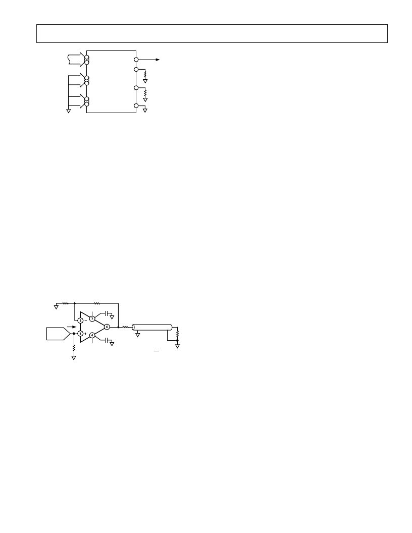
Figure 5. Input and Output Connections for Stand-Alone
Gray Scale or Composite Video
Video Output Buffers
The ADV7123 is specified to drive transmission line loads, as
are most monitors rated. The analog output configurations to
drive such loads are described in the Analog Interface section
and illustrated in Figure 5. However, in some applications it may
be required to drive long “transmission line” cable lengths. Cable
lengths greater than 10 meters can attenuate and distort high
frequency analog output pulses. The inclusion of output buffers
will compensate for some cable distortion. Buffers with large full
power bandwidths and gains between two and four will be required.
These buffers will also need to be able to supply sufficient current
over the complete output voltage swing. Analog Devices pro-
duces a range of suitable op amps for such applications. These
include the AD84x series of monolithic op amps. In very high
frequency applications (80 MHz), the AD8061 is recommended.
More information on line driver buffering circuits is given in the
relevant op amp data sheets.
Use of buffer amplifiers also allows implementation of other video
standards besides RS-343A and RS-170. Altering the gain compo-
nents of the buffer circuit will result in any desired video level.
AD848
0.1 F
IOR, IOG, IOB
Z
1
Z
2
Z
O
= 75
(CABLE)
Z
= 75
(SOURCE
TERMINATION)
Z
= 75
(MONITOR)
DACs
75
–V
S
+V
S
0.1 F
GAIN (G) = 1 +Z
1
Z
2
Figure 6. AD848 As an Output Buffer
PC Board Layout Considerations
The ADV7123 is optimally designed for lowest noise perfor-
mance, both radiated and conducted noise. To complement the
excellent noise performance of the ADV7123, it is imperative
that great care be given to the PC board layout. Figure 7
shows a recommended connection diagram for the ADV7123.
The layout should be optimized for lowest noise on the ADV7123
power and ground lines. This can be achieved by shielding the
digital inputs and providing good decoupling. The lead length
between groups of V
AA
and GND pins should be shortened to
minimize inductive ringing.
相關PDF資料 |
PDF描述 |
|---|---|
| ADV7123JST240 | CMOS, 240 MHz Triple 10-Bit High Speed Video DAC |
| ADV7123 | CMOS, 240 MHz Triple 10-Bit High Speed Video DAC(240MHz三通道10位高速視頻D/A轉換器) |
| ADV7125JST240 | CMOS, 330 MHz Triple 8-Bit High Speed Video DAC |
| ADV7125JST330 | CMOS, 330 MHz Triple 8-Bit High Speed Video DAC |
| ADV7125 | CMOS, 330 MHz Triple 8-Bit High Speed Video DAC |
相關代理商/技術參數 |
參數描述 |
|---|---|
| ADV7123JSTZ240 | 功能描述:IC DAC VIDEO TRPL HI SPD 48-LQFP RoHS:是 類別:集成電路 (IC) >> 數據采集 - 數模轉換器 系列:- 產品培訓模塊:Lead (SnPb) Finish for COTS Obsolescence Mitigation Program 標準包裝:50 系列:- 設置時間:4µs 位數:12 數據接口:串行 轉換器數目:2 電壓電源:單電源 功率耗散(最大):- 工作溫度:-40°C ~ 85°C 安裝類型:表面貼裝 封裝/外殼:8-TSSOP,8-MSOP(0.118",3.00mm 寬) 供應商設備封裝:8-uMAX 包裝:管件 輸出數目和類型:2 電壓,單極 采樣率(每秒):* 產品目錄頁面:1398 (CN2011-ZH PDF) |
| ADV7123JSTZ240 | 制造商:Analog Devices 功能描述:D/A Converter (D-A) IC |
| ADV7123JSTZ240-RL | 功能描述:IC DAC VIDEO 3-CH 240MHZ 48LQFP RoHS:是 類別:集成電路 (IC) >> 數據采集 - 數模轉換器 系列:- 標準包裝:47 系列:- 設置時間:2µs 位數:14 數據接口:并聯 轉換器數目:1 電壓電源:單電源 功率耗散(最大):55µW 工作溫度:-40°C ~ 85°C 安裝類型:表面貼裝 封裝/外殼:28-SSOP(0.209",5.30mm 寬) 供應商設備封裝:28-SSOP 包裝:管件 輸出數目和類型:1 電流,單極;1 電流,雙極 采樣率(每秒):* |
| ADV7123JSTZ240TMP | 制造商:Analog Devices 功能描述: |
| ADV7123JSTZ330 | 功能描述:IC DAC VIDEO 3CH 330MHZ 48-LQFP RoHS:是 類別:集成電路 (IC) >> 數據采集 - 數模轉換器 系列:- 產品培訓模塊:Lead (SnPb) Finish for COTS Obsolescence Mitigation Program 標準包裝:50 系列:- 設置時間:4µs 位數:12 數據接口:串行 轉換器數目:2 電壓電源:單電源 功率耗散(最大):- 工作溫度:-40°C ~ 85°C 安裝類型:表面貼裝 封裝/外殼:8-TSSOP,8-MSOP(0.118",3.00mm 寬) 供應商設備封裝:8-uMAX 包裝:管件 輸出數目和類型:2 電壓,單極 采樣率(每秒):* 產品目錄頁面:1398 (CN2011-ZH PDF) |
發布緊急采購,3分鐘左右您將得到回復。