- 您現(xiàn)在的位置:買賣IC網(wǎng) > PDF目錄374046 > ADV7172KST (ANALOG DEVICES INC) Digital PAL/NTSC Video Encoder with Six DACs 10 Bits, Color Control and Enhanced Power Management PDF資料下載
參數(shù)資料
| 型號: | ADV7172KST |
| 廠商: | ANALOG DEVICES INC |
| 元件分類: | 顏色信號轉換 |
| 英文描述: | Digital PAL/NTSC Video Encoder with Six DACs 10 Bits, Color Control and Enhanced Power Management |
| 中文描述: | COLOR SIGNAL ENCODER, PQFP48 |
| 封裝: | PLASTIC, TQFP-48 |
| 文件頁數(shù): | 23/59頁 |
| 文件大小: | 455K |
| 代理商: | ADV7172KST |
第1頁第2頁第3頁第4頁第5頁第6頁第7頁第8頁第9頁第10頁第11頁第12頁第13頁第14頁第15頁第16頁第17頁第18頁第19頁第20頁第21頁第22頁當前第23頁第24頁第25頁第26頁第27頁第28頁第29頁第30頁第31頁第32頁第33頁第34頁第35頁第36頁第37頁第38頁第39頁第40頁第41頁第42頁第43頁第44頁第45頁第46頁第47頁第48頁第49頁第50頁第51頁第52頁第53頁第54頁第55頁第56頁第57頁第58頁第59頁
ADV7172/ADV7173
–23–
REV. A
OUTPUT VIDEO TIMING
The video timing generator generates the appropriate sync,
blank and burst sequence that controls the output analog wave-
forms. These sequences are summarized below. In slave modes,
the following sequences are synchronized with the input timing
control signals. In master modes, the timing generator free runs
and generates the following sequences in addition to the output
timing control signals.
NTSC–Interlaced:
Scan Lines 1–9 and 264–272 are always
blanked and vertical sync pulses are included. Scan Lines 525,
10–21 and 262, 263, 273-284 are also blanked and can be used
for closed captioning data. Burst is disabled on Lines 1–6, 261–
269 and 523–525.
NTSC–Noninterlaced:
Scan Lines 1–9 are always blanked
and vertical sync pulses are included. Scan Lines 10–21 are also
blanked and can be used for closed captioning data. Burst is
disabled on Lines 1–6, 261–262.
PAL–Interlaced:
Scan Lines 1–6, 311–318 and 624–625 are
always blanked and vertical sync pulses are included in Fields 1,
2, 5 and 6. Scan Lines 1–5, 311–319 and 624–625 are always
blanked and vertical sync pulses are included in Fields 3, 4, 7
and 8. The remaining scan lines in the vertical blanking interval
are also blanked and can be used for teletext data. Burst is dis-
abled on Lines 1–6, 311–318 and 623–625 in Fields 1, 2, 5 and
6. Burst is disabled on Lines 1–5, 311–319 and 623–625 in
Fields 3, 4, 7 and 8.
PAL–Noninterlaced
: Scan Lines 1–6 and 311–312 are always
blanked and vertical sync pulses are included. The remaining
scan lines in the vertical blanking interval are also blanked and
can be used for teletext data. Burst is disabled on Lines 1–5,
310–312.
POWER-ON RESET
After power-up, it is necessary to execute a reset operation. A
reset occurs on the falling edge of a high-to-low transition on
the
RESET
pin. This initializes the pixel port such that the pixel
inputs P7–P0 are not selected. After reset, the ADV7172/
ADV7173 is automatically set up to operate in NTSC/PAL
mode, depending on the PAL_NTSC pin. The subcarrier fre-
quency registers are automatically loaded with the correct values
for PAL or NTSC. All other registers, with the exception of
Mode Registers 1 and 2, are set to 00H. Mode Register 1 is set
to 07H. This is to ensure DACs D, E and F are ON after
power-up. All bits of Mode Register 2 are set to “0,” with the
exception of Bit 3 (i.e., Mode Register 2 reads 08H). Bit MR23
of Mode Register 2 is set to Logic “1.” This enables the 7.5 IRE
pedestal.
RESET SEQUENCE
When
RESET
becomes active, the ADV7172/ADV7173 reverts
to the default output configuration. DACs A, B, C are off and
DACs D, E, F are powered on and output composite, luma and
chroma signals respectively. Mode Register 2, Bit 6 (MR26),
resets to “0.” The ADV7172/ADV7173 internal timing is under
the control of the logic level on the NTSC_PAL pin.
When
RESET
is released Y, Cr, Cb values corresponding to a
black screen are input to the ADV7172/ADV7173. Output
timing signals are still suppressed at this stage.
When the user requires valid data, MR26 is set to “1” to allow
the valid pixel data to pass through the encoder. Digital output
timing signals become active and the encoder timing is now
under the control of the timing registers. If, at this stage, the
user wishes to select a video standard different from that on
the NTSC_PAL pin, Mode Register 2, Bit 5 (MR25) is set
(“1”) and the video standard required is selected by program-
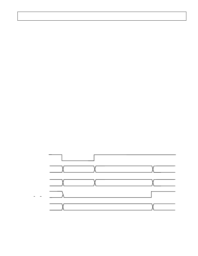
ming Mode Register 0. Figure 36 illustrates the reset sequence
timing.
XXXXXXX
XXXXXXX
XXXXXXX
XXXXXXX
DIGITAL TIMING SIGNALS SUPPRESSED
BLACK VALUE
BLACK VALUE WITH SYNC
VALID VIDEO
VALID VIDEO
0
1
TIMING ACTIVE
RESET
COMPOSITE/Y
CHROMA
MR26
PIXEL DATA VALID
DIGITAL TIMING
0
512
Figure 36.
RESET
Sequence Timing Diagram
相關PDF資料 |
PDF描述 |
|---|---|
| ADV7172 | Digital PAL/NTSC Video Encoder with Six DACs 10 Bits, Color Control and Enhanced Power Management |
| ADV7173 | Digital PAL/NTSC Video Encoder with Six DACs 10 Bits, Color Control and Enhanced Power Management |
| ADV7173* | Digital PAL/NTSC Video Encoder with Six DACs (10 Bits). Color Control and Enhanced Power Management |
| ADV7174 | Chip Scale PAL/NTSC Video Encoder with Advanced Power Management |
| ADV7174BCP | Chip Scale PAL/NTSC Video Encoder with Advanced Power Management |
相關代理商/技術參數(shù) |
參數(shù)描述 |
|---|---|
| ADV7172KST-REEL | 制造商:Analog Devices 功能描述: |
| ADV7172KSTZ | 制造商:Analog Devices 功能描述: |
| ADV7172KSTZ-REEL | 功能描述:IC DAC VIDEO NTSC 6-CH 48-LQFP RoHS:是 類別:集成電路 (IC) >> 接口 - 編碼器,解碼器,轉換器 系列:- 產(chǎn)品變化通告:Development Systems Discontinuation 26/Apr/2011 標準包裝:1 系列:- 類型:編碼器 應用:DVB-S.2 系統(tǒng) 電壓 - 電源,模擬:- 電壓 - 電源,數(shù)字:- 安裝類型:- 封裝/外殼:模塊 供應商設備封裝:模塊 包裝:散裝 其它名稱:Q4645799 |
| ADV7173 | 制造商:AD 制造商全稱:Analog Devices 功能描述:Digital PAL/NTSC Video Encoder with Six DACs 10 Bits, Color Control and Enhanced Power Management |
發(fā)布緊急采購,3分鐘左右您將得到回復。