- 您現在的位置:買賣IC網 > PDF目錄374046 > ADV7178KS (ANALOG DEVICES INC) Integrated Digital CCIR-601 to PAL/NTSC Video Encoder PDF資料下載
參數資料
| 型號: | ADV7178KS |
| 廠商: | ANALOG DEVICES INC |
| 元件分類: | 顏色信號轉換 |
| 英文描述: | Integrated Digital CCIR-601 to PAL/NTSC Video Encoder |
| 中文描述: | COLOR SIGNAL ENCODER, PQFP44 |
| 封裝: | PLASTIC, MO-112-AA-1, MQFP-44 |
| 文件頁數: | 27/38頁 |
| 文件大小: | 280K |
| 代理商: | ADV7178KS |
第1頁第2頁第3頁第4頁第5頁第6頁第7頁第8頁第9頁第10頁第11頁第12頁第13頁第14頁第15頁第16頁第17頁第18頁第19頁第20頁第21頁第22頁第23頁第24頁第25頁第26頁當前第27頁第28頁第29頁第30頁第31頁第32頁第33頁第34頁第35頁第36頁第37頁第38頁
ADV7177/ADV7178
–27–
REV. 0
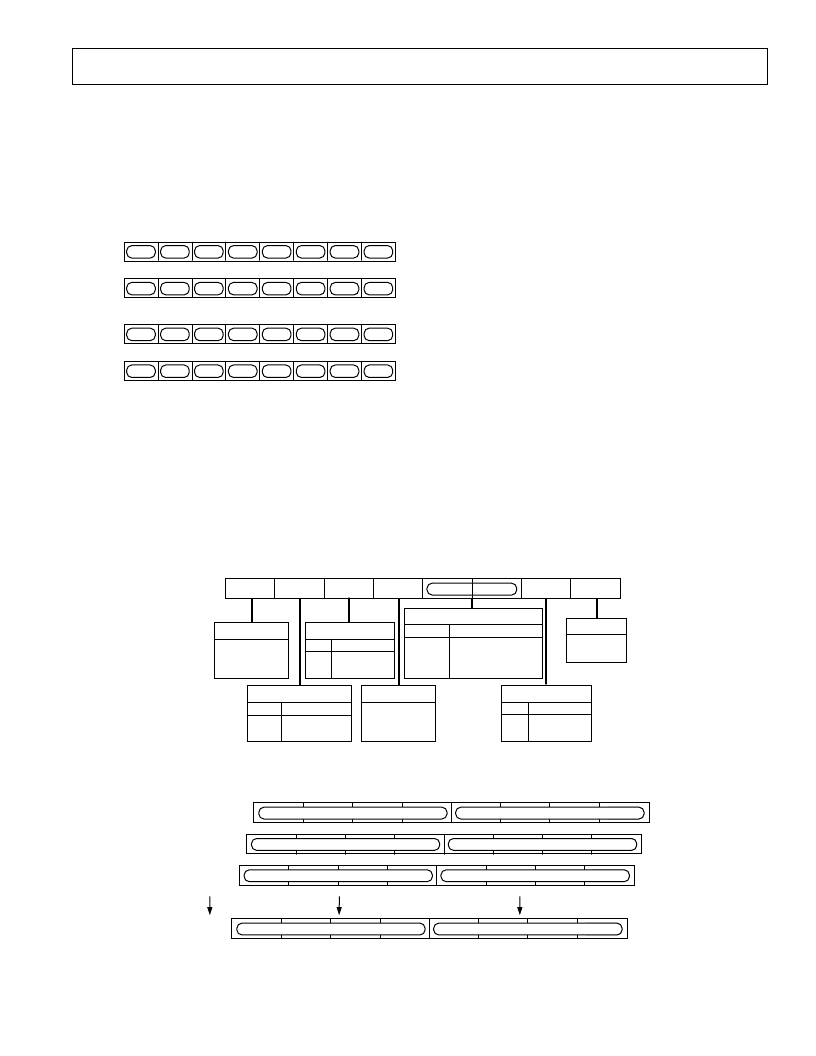
NTSC PEDESTAL REGISTERS 3–0 (PCE15–0, PCO15–0)
(Subaddress [SR4–SR0] = 11–0EH)
These 8-bit-wide registers are used to set up the NTSC pedestal
on a line-by-line basis in the vertical blanking interval for both
odd and even fields. Figure 40 show the four control registers.
A Logic “1” in any of the bits of these registers has the effect of
turning the pedestal OFF on the equivalent line when used in
NTSC.
FIELD 1/3
PCO6
PCO5
PCO3
PCO1
PCO4
PCO2
PCO0
PCO7
LINE 17 LINE 16 LINE 15 LINE 14 LINE 13 LINE 12 LINE 11 LINE 10
PCO14
PCO13
PCO11
PCO9
PCO12
PCO10
PCO8
PCO15
LINE 25 LINE 24 LINE 23 LINE 22 LINE 21 LINE 20 LINE 19 LINE 18
FIELD 1/3
FIELD 2/4
PCE6
PCE5
PCE3
PCE1
PCE4
PCE2
PCE0
PCE7
LINE 17 LINE 16 LINE 15 LINE 14 LINE 13 LINE 12 LINE 11 LINE 10
PCE14
PCE13
PCE11
PCE9
PCE12
PCE10
PCE8
PCE15
LINE 25 LINE 24 LINE 23 LINE 22 LINE 21 LINE 20 LINE 19 LINE 18
FIELD 2/4
Figure 40. Pedestal Control Registers
MODE REGISTER 3 MR3 (MR37–MR30)
(Address [SR4–SR0] = 12H)
Mode Register 3 is an 8-bit-wide register.
Figure 41 shows the various operations under the control of
Mode Register 3.
MR3 BIT DESCRIPTION
Revision Code (MR30)
This bit is read only and indicates the revision of the device.
VBI Pass-Through Control (MR31)
This bit determines whether or not data in the vertical blanking
interval (VBI) is output to the analog outputs or blanked.
Clock Output Select (MR33–MR32)
These bits control the synchronous clock output signal. The
clock can be 27 MHz, 13.5 MHz or disabled, depending on the
values of these bits.
OSD Enable (MR35)
A logic one in MR35 will enable the OSD function on the
ADV7177.
Reserved (MR36)
These bits are reserved.
Input Default Color (MR36)
This bit determines the default output color from the DACs for
zero input data (or disconnected). A Logical “0” means that the
color corresponding to 00000000 will be displayed. A Logical
“1” forces the output color to black for 00000000 input video
data.
OSD REGISTER 0–11
(Address [SR4–SR0] = 12H–1DH)
There are 12 OSD registers as shown in Figure 42. There are
four bits for each Y, Cb and Cr value, there are four zero added
to give the complete byte for each value loaded internally.
(Y0 = [Y0
3
, Y0
2
, Y0
1
, Y0
0
, 0, 0, 0, 0], Cb = [Cb
3
, Cb
2
, Cb
1
,
Cb
0
, 0, 0, 0, 0,], Cr = [Cr
3
, Cr
2
, Cr
1
, Cr
0
, 0, 0, 0, 0].)
MR31
MR30
MR37
MR32
MR34
MR33
MR35
MR36
ZERO SHOULD
BE WRITTEN TO
THIS BIT
MR34
INPUT DEFAULT COLOR
0
1
INPUT COLOR
BLACK
MR36
VBI PASSTHROUGH
0 DISABLE
1 ENABLE
MR31
CLOCK CONTROL
0
0
1
1
0
1
0
1
CLOCK OUTPUT OFF
13.5MHz OUTPUT
27MHz OUTPUT
CLOCK OUTPUT OFF
MR33-32
MR30
REV CODE
(READ ONLY)
ZERO SHOULD
BE WRITTEN TO
THIS BIT
MR37
OSD ENABLE
0 DISABLE
1 ENABLE
MR35
Figure 41. Mode Register 3
Y0
Cr0
Cb0
Y1
Cr1
Cb1
Cr7
Cb7
OSD
REG 0
OSD
REG 1
OSD
REG 2
OSD
REG 11
Figure 42. OSD Registers
相關PDF資料 |
PDF描述 |
|---|---|
| ADV7180 | 10-Bit, 4 x Oversampling SDTV Video Decoder |
| ADV7180BCPZ | 10-Bit, 4 x Oversampling SDTV Video Decoder |
| ADV7180BSTZ | 10-Bit, 4 x Oversampling SDTV Video Decoder |
| ADV7181 | Multiformat SDTV Video Decoder |
| ADV7181B | Multiformat SDTV Video Decoder |
相關代理商/技術參數 |
參數描述 |
|---|---|
| ADV7178KS-REEL | 制造商:Analog Devices 功能描述: |
| ADV7179 | 制造商:AD 制造商全稱:Analog Devices 功能描述:Chip Scale PAL/NTSC Video Encoder with Advanced Power Management |
| ADV7179BCP | 制造商:Analog Devices 功能描述:Video Encoder 3DAC 10-Bit 40-Pin LFCSP EP 制造商:Analog Devices 功能描述:IC VIDEO ENCODER |
| ADV7179BCP1 | 制造商:AD 制造商全稱:Analog Devices 功能描述:Chip Scale PAL/NTSC Video Encoder with Advanced Power Management |
| ADV7179BCP-REEL | 制造商:Analog Devices 功能描述:Video Encoder 3DAC 10-Bit 40-Pin LFCSP EP T/R |
發布緊急采購,3分鐘左右您將得到回復。