- 您現(xiàn)在的位置:買賣IC網(wǎng) > PDF目錄48365 > AOD403 (ALPHA AND OMEGA SEMICONDUCTOR) 70 A, 30 V, 0.008 ohm, P-CHANNEL, Si, POWER, MOSFET, TO-252 PDF資料下載
參數(shù)資料
| 型號(hào): | AOD403 |
| 廠商: | ALPHA AND OMEGA SEMICONDUCTOR |
| 元件分類: | JFETs |
| 英文描述: | 70 A, 30 V, 0.008 ohm, P-CHANNEL, Si, POWER, MOSFET, TO-252 |
| 封裝: | GREEN, DPAK-3 |
| 文件頁數(shù): | 2/6頁 |
| 文件大小: | 505K |
| 代理商: | AOD403 |
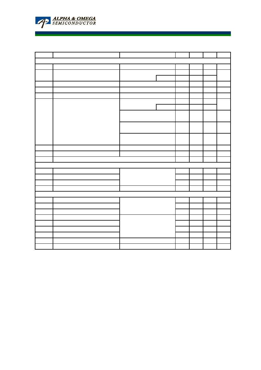
AOD403/AOI403
Symbol
Min
Typ
Max
Units
BVDSS
-30
V
VDS=-30V, VGS=0V
-1
TJ=55°C
-5
IGSS
±100
nA
VGS(th)
Gate Threshold Voltage
-1.5
-2.5
-3.5
V
ID(ON)
-200
A
5.1
6.2
TJ=125°C
7.6
9.2
gFS
42
S
VSD
-0.7
-1
V
IS
-70
A
Ciss
2310
2890
3500
pF
Coss
410
585
760
pF
Crss
280
470
660
pF
Rg
1.9
3.8
5.7
Q
40
51
61
nC
VGS=0V, VDS=-15V, f=1MHz
SWITCHING PARAMETERS
Electrical Characteristics (TJ=25°C unless otherwise noted)
STATIC PARAMETERS
Parameter
Conditions
Drain-Source Breakdown Voltage
ID=-250A, VGS=0V
VGS=-10V, VDS=-5V
VGS=-20V, ID=-20A
Forward Transconductance
Diode Forward Voltage
VGS=-10V, ID=-20A
TO252
IS=-1A,VGS=0V
VDS=-5V, ID=-20A
On state drain current
Static Drain-Source On-Resistance
VGS=-10V, ID=-20A
TO251A
IDSS
A
VDS=VGS ID=-250A
VDS=0V, VGS= ±25V
Zero Gate Voltage Drain Current
Gate-Body leakage current
m
TO252
6.2
8
m
VGS=-20V, ID=-20A
TO251A
Gate resistance
VGS=0V, VDS=0V, f=1MHz
Total Gate Charge
Reverse Transfer Capacitance
Maximum Body-Diode Continuous Current
G
Input Capacitance
Output Capacitance
DYNAMIC PARAMETERS
RDS(ON)
m
m
5.6
6.7
8.5
Qg
40
51
61
nC
Qgs
10
12
14
nC
Qgd
10
16
22
nC
tD(on)
16
ns
tr
12
ns
tD(off)
45
ns
tf
22
ns
trr
14
18
22
ns
Qrr
9
11
13
nC
THIS PRODUCT HAS BEEN DESIGNED AND QUALIFIED FOR THE CONSUMER MARKET. APPLICATIONS OR USES AS CRITICAL
COMPONENTS IN LIFE SUPPORT DEVICES OR SYSTEMS ARE NOT AUTHORIZED. AOS DOES NOT ASSUME ANY LIABILITY ARISING
OUT OF SUCH APPLICATIONS OR USES OF ITS PRODUCTS. AOS RESERVES THE RIGHT TO IMPROVE PRODUCT DESIGN,
FUNCTIONS AND RELIABILITY WITHOUT NOTICE.
IF=-20A, dI/dt=100A/s
Body Diode Reverse Recovery Time
Turn-Off Fall Time
Total Gate Charge
VGS=-10V, VDS=-15V, ID=-20A
Gate Source Charge
Gate Drain Charge
VGS=-10V, VDS=-15V, RL=0.75,
RGEN=3
Turn-Off DelayTime
Body Diode Reverse Recovery Charge IF=-20A, dI/dt=100A/s
Turn-On DelayTime
Turn-On Rise Time
A. The value of RθJA is measured with the device mounted on 1in
2 FR-4 board with 2oz. Copper, in a still air environment with T
A =25°C. The
Power dissipation P
DSM is based on R
θJA and the maximum allowed junction temperature of 150°C. The value in any given application depends
on the user's specific board design, and the maximum temperature of 175°C may be used if the PCB allows it.
B. The power dissipation P
D is based on TJ(MAX)=175°C, using junction-to-case thermal resistance, and is more useful in setting the upper
dissipation limit for cases where additional heatsinking is used.
C. Repetitive rating, pulse width limited by junction temperature T
J(MAX)=175°C. Ratings are based on low frequency and duty cycles to keep initial
T
J =25°C.
D. The RθJA is the sum of the thermal impedence from junction to case RθJC and case to ambient.
E. The static characteristics in Figures 1 to 6 are obtained using <300
s pulses, duty cycle 0.5% max.
F. These curves are based on the junction-to-case thermal impedence which is measured with the device mounted to a large heatsink, assuming a
maximum junction temperature of T
J(MAX)=175°C. The SOA curve provides a single pulse rating.
G. The maximum current rating is package limited.
H. These tests are performed with the device mounted on 1 in2 FR-4 board with 2oz. Copper, in a still air environment with T
A=25°C.
Rev 8: May 2011
www.aosmd.com
Page 2 of 6
相關(guān)PDF資料 |
PDF描述 |
|---|---|
| AOI472A | 50 A, 25 V, 0.0052 ohm, N-CHANNEL, Si, POWER, MOSFET, TO-251 |
| AOL1426 | 46 A, 30 V, 0.0135 ohm, N-CHANNEL, Si, POWER, MOSFET |
| AON6704 | 85 A, 30 V, 0.0034 ohm, N-CHANNEL, Si, POWER, MOSFET |
| AON6718 | 80 A, 30 V, 0.005 ohm, N-CHANNEL, Si, POWER, MOSFET |
| AP01N40J | 0.5 A, 400 V, 16 ohm, N-CHANNEL, Si, POWER, MOSFET, TO-251 |
相關(guān)代理商/技術(shù)參數(shù) |
參數(shù)描述 |
|---|---|
| AOD403_030 | 功能描述:MOSFET P-CH TO252 制造商:alpha & omega semiconductor inc. 系列:- 包裝:帶卷(TR) 零件狀態(tài):停產(chǎn) FET 類型:P 溝道 技術(shù):MOSFET(金屬氧化物) 漏源電壓(Vdss):30V 電流 - 連續(xù)漏極(Id)(25°C 時(shí)):15A(Ta),70A(Tc) 驅(qū)動(dòng)電壓(最大 Rds On,最小 Rds On):10V,20V 不同 Id 時(shí)的 Vgs(th)(最大值):3.5V @ 250μA 不同 Vgs 時(shí)的柵極電荷?(Qg)(最大值):61nC @ 10V Vgs(最大值):±25V 不同 Vds 時(shí)的輸入電容(Ciss)(最大值):3500pF @ 15V FET 功能:- 功率耗散(最大值):2.5W(Ta),90W(Tc) 不同?Id,Vgs 時(shí)的?Rds On(最大值):6.2 毫歐 @ 20A,20V 工作溫度:-55°C ~ 175°C(TJ) 安裝類型:表面貼裝 供應(yīng)商器件封裝:TO-252 封裝/外殼:TO-252-3,DPak(2 引線 + 接片),SC-63 標(biāo)準(zhǔn)包裝:2,500 |
| AOD403_11 | 制造商:AOSMD 制造商全稱:Alpha & Omega Semiconductors 功能描述:30V P-Channel MOSFET |
| AOD403_13 | 制造商:AOSMD 制造商全稱:Alpha & Omega Semiconductors 功能描述:30V P-Channel MOSFET |
| AOD403_DELTA | 功能描述:MOSFET P-CH TO252 制造商:alpha & omega semiconductor inc. 系列:- 包裝:帶卷(TR) 零件狀態(tài):停產(chǎn) FET 類型:P 溝道 技術(shù):MOSFET(金屬氧化物) 漏源電壓(Vdss):30V 電流 - 連續(xù)漏極(Id)(25°C 時(shí)):15A(Ta),70A(Tc) 驅(qū)動(dòng)電壓(最大 Rds On,最小 Rds On):10V,20V 不同 Id 時(shí)的 Vgs(th)(最大值):3.5V @ 250μA 不同 Vgs 時(shí)的柵極電荷?(Qg)(最大值):61nC @ 10V Vgs(最大值):±25V 不同 Vds 時(shí)的輸入電容(Ciss)(最大值):3500pF @ 15V FET 功能:- 功率耗散(最大值):2.5W(Ta),90W(Tc) 不同?Id,Vgs 時(shí)的?Rds On(最大值):6.2 毫歐 @ 20A,20V 工作溫度:-55°C ~ 155°C(TJ) 安裝類型:表面貼裝 供應(yīng)商器件封裝:TO-252,(D-Pak) 封裝/外殼:TO-252-3,DPak(2 引線 + 接片),SC-63 標(biāo)準(zhǔn)包裝:2,500 |
| AOD403L | 制造商:AOSMD 制造商全稱:Alpha & Omega Semiconductors 功能描述:P-Channel Enhancement Mode Field Effect Transistor |
發(fā)布緊急采購,3分鐘左右您將得到回復(fù)。