- 您現(xiàn)在的位置:買賣IC網(wǎng) > PDF目錄22006 > EP4CE40F29I8LN (Altera)IC CYCLONE IV E FPGA 40K 780FBGA PDF資料下載
參數(shù)資料
| 型號(hào): | EP4CE40F29I8LN |
| 廠商: | Altera |
| 文件頁(yè)數(shù): | 20/42頁(yè) |
| 文件大小: | 0K |
| 描述: | IC CYCLONE IV E FPGA 40K 780FBGA |
| 產(chǎn)品培訓(xùn)模塊: | Designing an IP Surveillance Camera Three Reasons to Use FPGA's in Industrial Designs Cyclone IV FPGA Family Overview |
| 特色產(chǎn)品: | Cyclone? IV FPGAs |
| 標(biāo)準(zhǔn)包裝: | 36 |
| 系列: | CYCLONE® IV E |
| LAB/CLB數(shù): | 2475 |
| 邏輯元件/單元數(shù): | 39600 |
| RAM 位總計(jì): | 1161216 |
| 輸入/輸出數(shù): | 532 |
| 電源電壓: | 0.97 V ~ 1.03 V |
| 安裝類型: | 表面貼裝 |
| 工作溫度: | -40°C ~ 100°C |
| 封裝/外殼: | 780-BBGA |
| 供應(yīng)商設(shè)備封裝: | 780-FBGA(29x29) |
| 其它名稱: | 544-2684 |
第1頁(yè)第2頁(yè)第3頁(yè)第4頁(yè)第5頁(yè)第6頁(yè)第7頁(yè)第8頁(yè)第9頁(yè)第10頁(yè)第11頁(yè)第12頁(yè)第13頁(yè)第14頁(yè)第15頁(yè)第16頁(yè)第17頁(yè)第18頁(yè)第19頁(yè)當(dāng)前第20頁(yè)第21頁(yè)第22頁(yè)第23頁(yè)第24頁(yè)第25頁(yè)第26頁(yè)第27頁(yè)第28頁(yè)第29頁(yè)第30頁(yè)第31頁(yè)第32頁(yè)第33頁(yè)第34頁(yè)第35頁(yè)第36頁(yè)第37頁(yè)第38頁(yè)第39頁(yè)第40頁(yè)第41頁(yè)第42頁(yè)
Chapter 1: Cyclone IV Device Datasheet
1–27
Switching Characteristics
December 2013
Altera Corporation
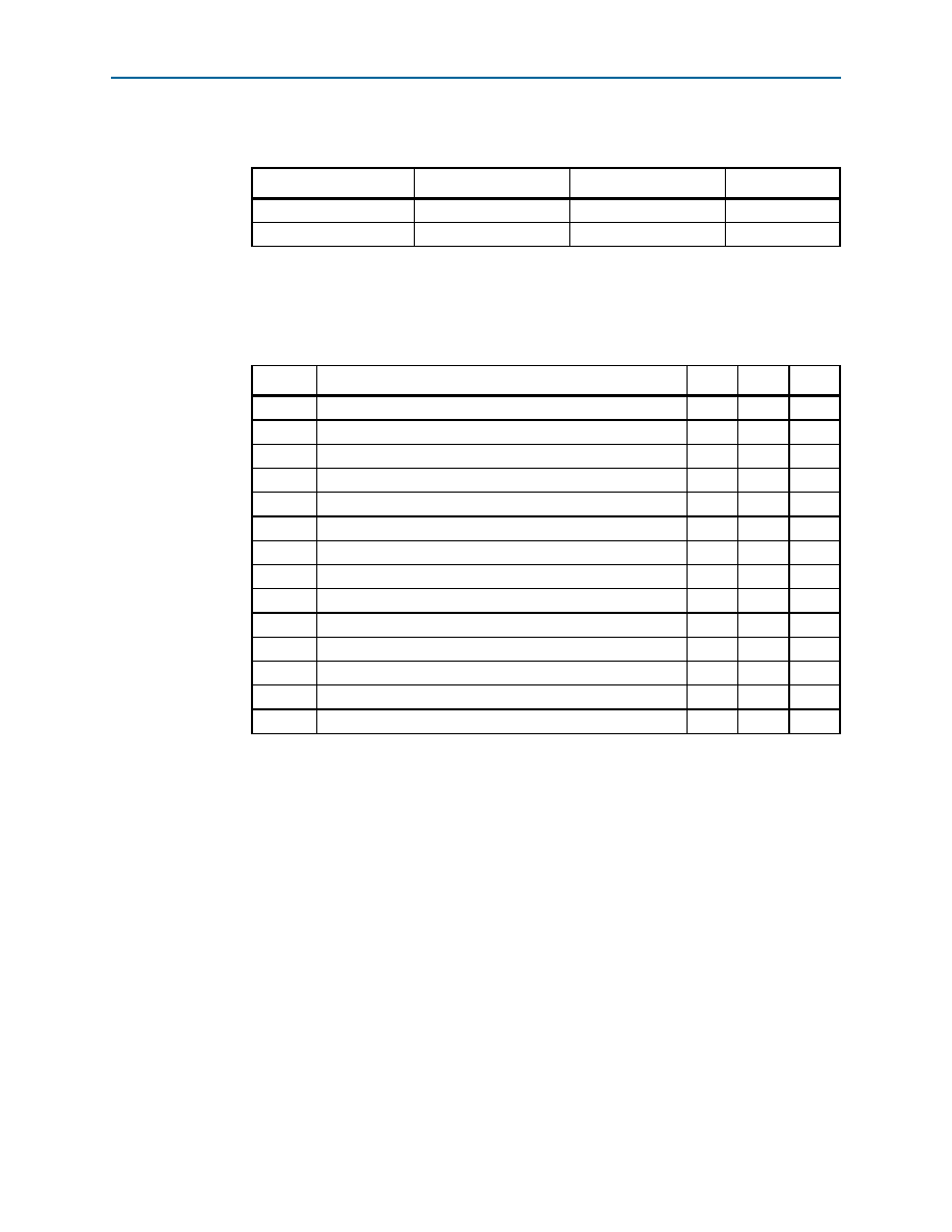
Table 1–29 lists the active configuration mode specifications for Cyclone IV devices.
Table 1–30 lists the JTAG timing parameters and values for Cyclone IV devices.
Periphery Performance
This section describes periphery performance, including high-speed I/O and external
memory interface.
I/O performance supports several system interfaces, such as the high-speed I/O
interface, external memory interface, and the PCI/PCI-X bus interface. I/Os using the
SSTL-18 Class I termination standard can achieve up to the stated DDR2 SDRAM
interfacing speeds. I/Os using general-purpose I/O standards such as 3.3-, 3.0-, 2.5-,
1.8-, or 1.5-LVTTL/LVCMOS are capable of a typical 200 MHz interfacing frequency
with a 10 pF load.
Table 1–29. Active Configuration Mode Specifications for Cyclone IV Devices
Programming Mode
DCLK Range
Typical DCLK
Unit
Active Parallel (AP) (1)
20 to 40
33
MHz
Active Serial (AS)
20 to 40
33
MHz
Note to Table 1–29:
(1) AP configuration mode is only supported for Cyclone IV E devices.
Table 1–30. JTAG Timing Parameters for Cyclone IV Devices (1)
Symbol
Parameter
Min
Max
Unit
tJCP
TCK clock period
40
—
ns
tJCH
TCK clock high time
19
—
ns
tJCL
TCK clock low time
19
—
ns
tJPSU_TDI
JTAG port setup time for TDI
1
—
ns
tJPSU_TMS JTAG port setup time for TMS
3
—
ns
tJPH
JTAG port hold time
10
—
ns
tJPCO
—15
ns
tJPZX
JTAG port high impedance to valid output (2), (3)
—15
ns
tJPXZ
JTAG port valid output to high impedance (2), (3)
—15
ns
tJSSU
Capture register setup time
5
—
ns
tJSH
Capture register hold time
10
—
ns
tJSCO
Update register clock to output
—
25
ns
tJSZX
Update register high impedance to valid output
—
25
ns
tJSXZ
Update register valid output to high impedance
—
25
ns
Notes to Table 1–30:
(1) For more information about JTAG waveforms, refer to “JTAG Waveform” in “Glossary” on page 1–37.
(2) The specification is shown for 3.3-, 3.0-, and 2.5-V LVTTL/LVCMOS operation of JTAG pins. For 1.8-V
LVTTL/LVCMOS and 1.5-V LVCMOS, the output time specification is 16 ns.
(3) For EP4CGX22, EP4CGX30 (F324 and smaller package), EP4CGX110, and EP4CGX150 devices, the output time
specification for 3.3-, 3.0-, and 2.5-V LVTTL/LVCMOS operation of JTAG pins is 16 ns. For 1.8-V LVTTL/LVCMOS
and 1.5-V LVCMOS, the output time specification is 18 ns.
相關(guān)PDF資料 |
PDF描述 |
|---|---|
| GEA18DTMI | CONN EDGECARD 36POS R/A .125 SLD |
| AGL1000V2-FGG256 | IC FPGA IGLOO 1.2-1.5V 256FPBGA |
| TAP107K006SRW | CAP TANT 100UF 6.3V 10% RADIAL |
| VE-273-CW-F2 | CONVERTER MOD DC/DC 24V 100W |
| 1624112-5 | INDUCTOR 33NH 600MA 0603 |
相關(guān)代理商/技術(shù)參數(shù) |
參數(shù)描述 |
|---|---|
| EP4CE40U19I7N | 功能描述:FPGA - 現(xiàn)場(chǎng)可編程門陣列 FPGA - Cyclone IV E 2475 LABs 328 IOs RoHS:否 制造商:Altera Corporation 系列:Cyclone V E 柵極數(shù)量: 邏輯塊數(shù)量:943 內(nèi)嵌式塊RAM - EBR:1956 kbit 輸入/輸出端數(shù)量:128 最大工作頻率:800 MHz 工作電源電壓:1.1 V 最大工作溫度:+ 70 C 安裝風(fēng)格:SMD/SMT 封裝 / 箱體:FBGA-256 |
| EP4CE55 | 制造商:ALTERA 制造商全稱:Altera Corporation 功能描述:Cyclone IV FPGA Device Family Overview |
| EP4CE55F17C8 | 制造商:ALTERA 制造商全稱:Altera Corporation 功能描述:Cyclone IV Device Datasheet |
| EP4CE55F23C6 | 功能描述:FPGA - 現(xiàn)場(chǎng)可編程門陣列 FPGA - Cyclone IV E 3491 LABs 324 IOs RoHS:否 制造商:Altera Corporation 系列:Cyclone V E 柵極數(shù)量: 邏輯塊數(shù)量:943 內(nèi)嵌式塊RAM - EBR:1956 kbit 輸入/輸出端數(shù)量:128 最大工作頻率:800 MHz 工作電源電壓:1.1 V 最大工作溫度:+ 70 C 安裝風(fēng)格:SMD/SMT 封裝 / 箱體:FBGA-256 |
| EP4CE55F23C6N | 功能描述:FPGA - 現(xiàn)場(chǎng)可編程門陣列 FPGA - Cyclone IV E 3491 LABs 324 IOs RoHS:否 制造商:Altera Corporation 系列:Cyclone V E 柵極數(shù)量: 邏輯塊數(shù)量:943 內(nèi)嵌式塊RAM - EBR:1956 kbit 輸入/輸出端數(shù)量:128 最大工作頻率:800 MHz 工作電源電壓:1.1 V 最大工作溫度:+ 70 C 安裝風(fēng)格:SMD/SMT 封裝 / 箱體:FBGA-256 |
發(fā)布緊急采購(gòu),3分鐘左右您將得到回復(fù)。