- 您現在的位置:買賣IC網 > PDF目錄375723 > FAN5059 (Fairchild Semiconductor Corporation) High Performance Programmable Synchronous PDF資料下載
參數資料
| 型號: | FAN5059 |
| 廠商: | Fairchild Semiconductor Corporation |
| 英文描述: | High Performance Programmable Synchronous |
| 中文描述: | 高性能可編程同步 |
| 文件頁數: | 2/18頁 |
| 文件大小: | 206K |
| 代理商: | FAN5059 |
FAN5059
PRODUCT SPECIFICATION
2
REV. 1.0.4 8/14/03
currents in excess of 16A from a 5V source with minimal
external circuitry. Synchronous-mode operation offers opti-
mum efficiency over the entire specified output voltage range.
An on-board precision low TC reference achieves tight toler-
ance voltage regulation without expensive external compo-
nents, while Programmable Active Droop
tailoring of voltage for the most demanding load transients. The
FAN5059 includes linear regulator controllers for Vtt termina-
tion (1.5V), Vclock (2.5V), and Vnorthbridge (1.8V) or Vagp
(selectable 1.5V/3.3V), each adjustable with an external divider.
The FAN5059 also offers integrated functions including Power
Good, Output Enable/Soft Start and current limiting, and is
available in a 24 pin SOIC package.
permits exact
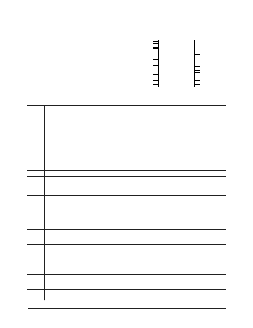
Pin Assignments
24
23
22
21
20
19
18
17
16
15
14
13
FAN5059
HIDRV
SW
GNDA
VID4
VID3
VID2
VID1
VID0
VTTGATE
VTTFB
VCKGATE
VCKFB
VCCP
LODRV
GNDP
VCCA
VFB
DROOP
ILIM
PWRGD
SS/ENABLE
TYPEDET
VAGPGATE
VAGPFB
1
2
3
4
5
6
7
8
9
10
11
12
Pin Definitions
Pin
Number Pin Name
1
Pin Function Description
High Side FET Driver.
MOSFET. The trace from this pin to the MOSFET gate should be <0.5".
High side Driver Source and Low side Driver Drain Switching Node.
DROOP and ILIM pins allows FET sensing for Vcc current.
Analog Ground.
Return path for low power analog circuitry. This pin should be
connected to a low impedance system ground plane to minimize ground loops.
Voltage Identification Code Inputs.
These open collector/TTL compatible inputs will
program the output voltage over the ranges specified in Table 2. Pull-up resistors are
internal to the controller.
Gate Driver for VTT Transistor.
For 1.5V output.
Voltage Feedback for VTT.
Gate Driver for VCK Transistor.
For 2.5V output.
Voltage Feedback for VCK.
Voltage Feedback for VAGP.
Gate Driver for VAGP Transistor.
For 3.3/1.5V output.
Type Detect.
Sets 3.3V or 1.5V for AGP.
Output Enable.
A logic LOW on this pin will disable all outputs. An internal current source
allows for open collector control. This pin also doubles as soft start for all outputs.
Power Good Flag.
An open collector output that will be logic LOW if any output voltage
is more than ±12% outside of the nominal output voltage setpoint.
Vcc Current Feedback.
Pin 18 is used in conjunction with pin 2 as the input for the Vcc
current feedback control loop. Layout of these traces is critical to system performance.
See Application Information for details.
Droop set.
Use this pin to set magnitude of active droop.
Vcc Voltage Feedback.
Pin 20 is used as the input for the Vcc voltage feedback control
loop. See Application Information for details regarding correct layout.
Analog VCC.
Connect to system 5V supply and decouple with a 0.1μF ceramic capacitor.
Power Ground.
Return pin for high currents flowing in pin 24 (VCCP).
Vcc Low Side FET Driver.
Connect this pin through a resistor to the gate of an N-channel
MOSFET for synchronous operation. The trace from this pin to the MOSFET gate should
be <0.5".
Power VCC.
For all FET drivers. Connect to system 12V supply through a 33
decouple with a 1μF ceramic capacitor.
HIDRV
Connect this pin through a resistor to the gate of an N-channel
2
SW
Together with
3
GNDA
4-8
VID0-4
9
10
11
12
13
14
15
16
VTTGATE
VTTFB
VCKGATE
VCKFB
VAGPFB
VAGPGATE
TYPEDET
ENABLE/SS
17
PWRGD
18
ILIM
19
20
DROOP
VFB
21
22
23
VCCA
GNDP
LODRV
24
VCCP
, and
相關PDF資料 |
PDF描述 |
|---|---|
| FAN5063 | ACPI Dual Switch Controller |
| FAN5063M | Power Supply Switching Circuit |
| FAN5066 | Ultra Low Voltage Synchronous DC-DC Controller |
| FAN5066M | |
| FAN5066MTC | |
相關代理商/技術參數 |
參數描述 |
|---|---|
| FAN5059_BBA3026B WAF | 制造商:Fairchild Semiconductor Corporation 功能描述: |
| FAN5059M | 功能描述:開關變換器、穩壓器與控制器 DC-DC Controller HP Programmable Sync RoHS:否 制造商:Texas Instruments 輸出電壓:1.2 V to 10 V 輸出電流:300 mA 輸出功率: 輸入電壓:3 V to 17 V 開關頻率:1 MHz 工作溫度范圍: 安裝風格:SMD/SMT 封裝 / 箱體:WSON-8 封裝:Reel |
| FAN5059M_Q | 功能描述:開關變換器、穩壓器與控制器 DC-DC Controller HP Programmable Sync RoHS:否 制造商:Texas Instruments 輸出電壓:1.2 V to 10 V 輸出電流:300 mA 輸出功率: 輸入電壓:3 V to 17 V 開關頻率:1 MHz 工作溫度范圍: 安裝風格:SMD/SMT 封裝 / 箱體:WSON-8 封裝:Reel |
| FAN5059MX | 功能描述:開關變換器、穩壓器與控制器 DC-DC Controller HP Programmable Sync RoHS:否 制造商:Texas Instruments 輸出電壓:1.2 V to 10 V 輸出電流:300 mA 輸出功率: 輸入電壓:3 V to 17 V 開關頻率:1 MHz 工作溫度范圍: 安裝風格:SMD/SMT 封裝 / 箱體:WSON-8 封裝:Reel |
| FAN5061 | 制造商:未知廠家 制造商全稱:未知廠家 功能描述:Current-Mode SMPS Controller |
發布緊急采購,3分鐘左右您將得到回復。