- 您現在的位置:買賣IC網 > PDF目錄375782 > FDS4953 (Microsemi Corporation) RES ARRAY 360 OHM 4TERM 2RES SMD PDF資料下載
參數資料
| 型號: | FDS4953 |
| 廠商: | Microsemi Corporation |
| 英文描述: | RES ARRAY 360 OHM 4TERM 2RES SMD |
| 中文描述: | 評估板 |
| 文件頁數: | 14/18頁 |
| 文件大小: | 339K |
| 代理商: | FDS4953 |
LXE1710 E
VALUATION
B
OARD
U
SER
G
UIDE
Microsemi
Linfinity Microelectronics Division
11861 Western Avenue, Garden Grove, CA. 92841, 714-898-8121, Fax: 714-893-2570
Page 14
Copyright
2000
Rev. 1.1, 2000-12-01
G
ATE
R
ESISTOR
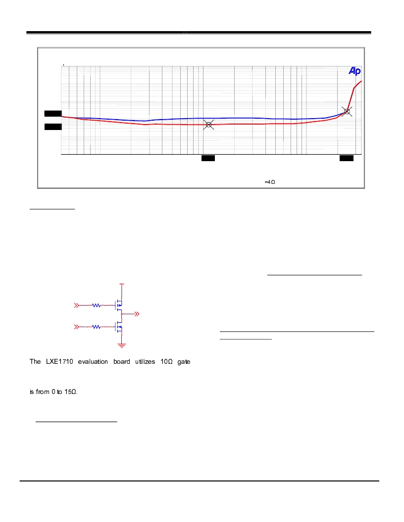
Series resistors (R6, R10, R11, R12) can be added to
the gate of MOSFETs (Q1 to Q4) to control the
switching transition times. This reduces signal
distortion as seen in the THD+N vs. Output Power
graph below. The slower switching speeds will
however, increase power dissipation and therefore
slightly decrease the overall efficiency of the amplifier.
P+
N+
OUT+
V
IN
Q1
Q2
R12
10
R11
10
- 3451
resistors, which improves (decreases) the THD+N
from 0.1% to 0.05% with a slight impact on efficiency
of approximately 2%. The recommended gate resistor
1 6!
O
SCILLATOR
C
ONFIGURATION
.
1 $
The oscillator is programmed by the external timing
components RPWM and CPWM. For a nominal
frequency of 333kHz, RPWM and CPWM should be
set to 49.9kOhms and 100pF respectively. Note that
in order to keep the slope of the PWM ramp voltage
proportional to the supply voltage, both the ramp peak
and valley voltages, and the charge and discharge
currents are proportional to the supply voltage. This
keeps the frequency relatively constant while keeping
the slope of the PWM ramp proportional to the voltage
on the VDD pin. For operating frequencies other than
333kHz, the frequency can be approximated by the
following equation:
ns
C
R
PWM
PWM
320
)
)(
)(
577
.
1
Frequency
+
=
M
ULTI
C
HANNEL
R
EQUIREMENTS AND
F
REQUENCY
S
YNCHRONIZATION
For applications that require more than a single
channel, the oscillators of multiple LX1710/1711
controllers can be configured for synchronous
operation. One unit, the master, is programmed for
the desired frequency with the RPWM and CPWM as
usual. Additional units will be slave units, and their
oscillators will be disabled by leaving the RPWM pin
disconnected. The CLOCK pin and the CPWM pin of
the slave units should be tied to the CLOCK pin and
the CPWM pin of the master unit respectively. In this
configuration, the CLOCK pins of the slave units begin
receiving instead of transmitting clock pulses. Also,
the CPWM pins quit driving the PWM capacitor in the
slave units. Note that for optimum performance, all
slave units should be located within a few inches of the
master unit.
Gate Resistor Impact On THD+N
0.001
100
20
0.005
0.01
0.1
1
2
10
50
0.26978
0.04675
T
50m
30
100m
200m
500m
1
2
5
10
20
24.56
1.131
Output Power (W)
f
IN
= 1kHz
No Gate Resistor
With 10
Gate Resistor
V
IN
= 15V
R
L
相關PDF資料 |
PDF描述 |
|---|---|
| FDS6612A | EVALUATION KIT |
| FDS4953 | Dual P-Channel, Logic Level, PowerTrenchTM MOSFET |
| FDS6612A | Single N-Channel, Logic Level, PowerTrenchTM MOSFET |
| FDS5170N7 | 60V N-Channel PowerTrench MOSFET |
| FDS5670 | 60V N-Channel PowerTrench⑩ MOSFET |
相關代理商/技術參數 |
參數描述 |
|---|---|
| FDS4953_02 | 制造商:FAIRCHILD 制造商全稱:Fairchild Semiconductor 功能描述:Dual 30V P-Channel PowerTrench MOSFET |
| FDS5170N7 | 功能描述:MOSFET 60V N-Ch PowerTrench RoHS:否 制造商:STMicroelectronics 晶體管極性:N-Channel 汲極/源極擊穿電壓:650 V 閘/源擊穿電壓:25 V 漏極連續電流:130 A 電阻汲極/源極 RDS(導通):0.014 Ohms 配置:Single 最大工作溫度: 安裝風格:Through Hole 封裝 / 箱體:Max247 封裝:Tube |
| FDS5351 | 功能描述:MOSFET 60V N-Channel PowerTrench RoHS:否 制造商:STMicroelectronics 晶體管極性:N-Channel 汲極/源極擊穿電壓:650 V 閘/源擊穿電壓:25 V 漏極連續電流:130 A 電阻汲極/源極 RDS(導通):0.014 Ohms 配置:Single 最大工作溫度: 安裝風格:Through Hole 封裝 / 箱體:Max247 封裝:Tube |
| FDS5670 | 功能描述:MOSFET SO-8 N-CH 60V RoHS:否 制造商:STMicroelectronics 晶體管極性:N-Channel 汲極/源極擊穿電壓:650 V 閘/源擊穿電壓:25 V 漏極連續電流:130 A 電阻汲極/源極 RDS(導通):0.014 Ohms 配置:Single 最大工作溫度: 安裝風格:Through Hole 封裝 / 箱體:Max247 封裝:Tube |
| FDS5670 | 制造商:Fairchild Semiconductor Corporation 功能描述:MOSFET N SO-8 |
發布緊急采購,3分鐘左右您將得到回復。