- 您現在的位置:買賣IC網 > PDF目錄375782 > FDS6644 (FAIRCHILD SEMICONDUCTOR CORP) 30V N-Channel PowerTrench MOSFET PDF資料下載
參數資料
| 型號: | FDS6644 |
| 廠商: | FAIRCHILD SEMICONDUCTOR CORP |
| 元件分類: | 小信號晶體管 |
| 英文描述: | 30V N-Channel PowerTrench MOSFET |
| 中文描述: | 13000 mA, 30 V, N-CHANNEL, Si, SMALL SIGNAL, MOSFET |
| 封裝: | SO-8 |
| 文件頁數: | 2/5頁 |
| 文件大小: | 79K |
| 代理商: | FDS6644 |
FDS6644 Rev A(W)
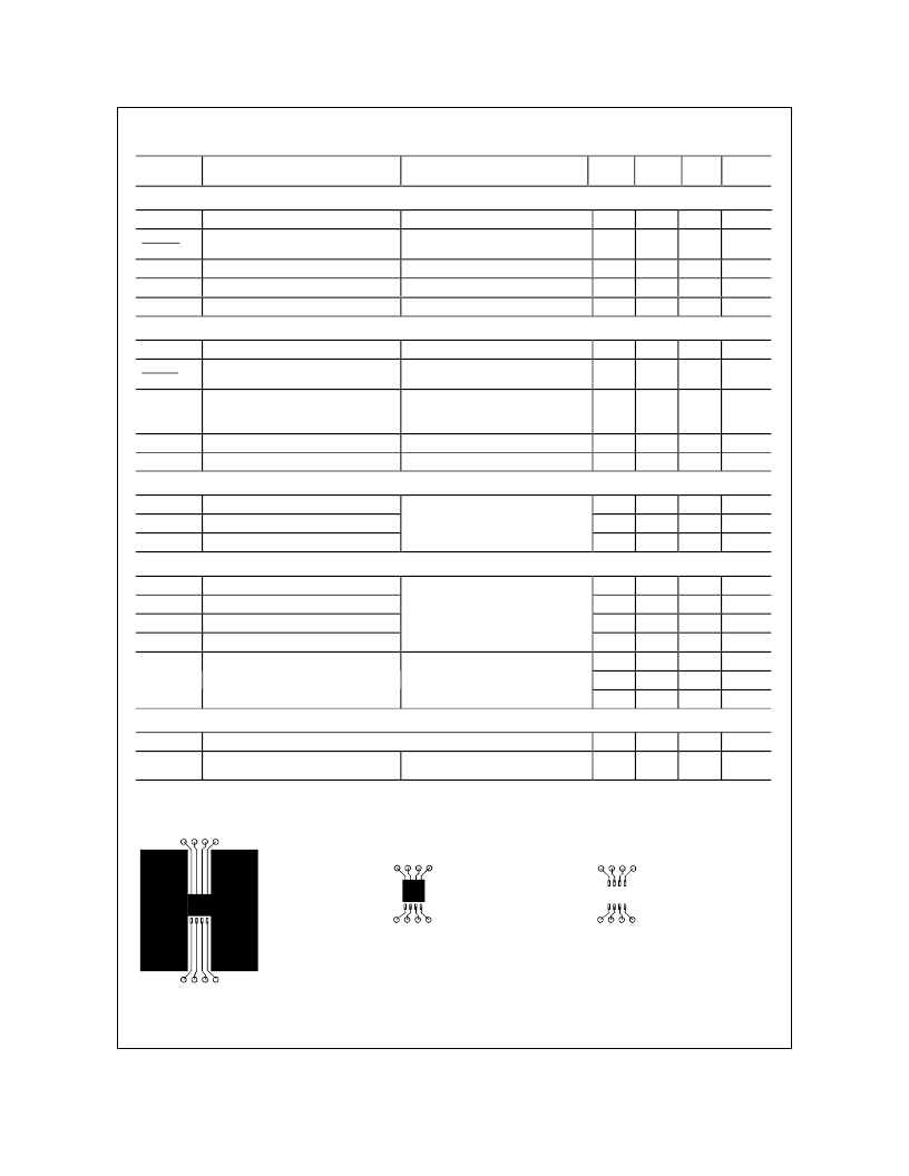
Electrical Characteristics
Symbol
T
A
= 25°C unless otherwise noted
Test Conditions
Parameter
Min
Typ
Max Units
Off Characteristics
BV
DSS
Drain–Source Breakdown Voltage
BV
DSS
T
J
Coefficient
I
DSS
Zero Gate Voltage Drain Current
I
GSSF
Gate–Body Leakage, Forward
I
GSSR
Gate–Body Leakage, Reverse
V
GS
= 0 V, I
D
= 250
μ
A
30
V
Breakdown Voltage Temperature
I
D
= 250
μ
A, Referenced to 25
°
C
27
mV/
°
C
V
DS
= 24 V, V
GS
= 0 V
V
GS
= 16 V, V
DS
= 0 V
V
GS
= –16 V, V
DS
= 0 V
1
μ
A
nA
nA
100
–100
On Characteristics
V
GS(th)
Gate Threshold Voltage
V
GS(th)
T
J
Temperature Coefficient
R
DS(on)
Static Drain–Source
On–Resistance
(Note 2)
V
DS
= V
GS
, I
D
= 250
μ
A
1
1.5
3
V
Gate Threshold Voltage
I
D
= 250
μ
A, Referenced to 25
°
C
–5
mV/
°
C
V
GS
= 10 V, I
D
= 13 A
V
GS
= 4.5 V, I
D
= 11.8 A
V
GS
= 10 V, I
D
= 13 A,T
J
=125
°
C
V
GS
= 10 V, V
DS
= 5 V
V
DS
= 5 V, I
D
= 13 A
6.5
7.5
10
8.5
10.5
13
m
I
D(on)
g
FS
Dynamic Characteristics
C
iss
Input Capacitance
C
oss
Output Capacitance
C
rss
Reverse Transfer Capacitance
On–State Drain Current
Forward Transconductance
26
A
S
74
3087
489
185
pF
pF
pF
V
DS
= 15 V, V
GS
= 0 V,
f = 1.0 MHz
Switching Characteristics
t
d(on)
Turn–On Delay Time
t
r
Turn–On Rise Time
t
d(off)
Turn–Off Delay Time
t
f
Turn–Off Fall Time
Q
g
Total Gate Charge
Q
gs
Gate–Source Charge
Q
gd
Gate–Drain Charge
Drain–Source Diode Characteristics and Maximum Ratings
I
S
Maximum Continuous Drain–Source Diode Forward Current
Drain–Source Diode Forward
Voltage
(Note 2)
10
12
48
10
25
7.5
6.5
20
22
77
20
35
ns
ns
ns
ns
nC
nC
nC
V
DD
= 15 V, I
D
= 1 A,
V
GS
= 10 V, R
GEN
= 6
V
DS
= 15 V, I
D
= 13 A,
V
GS
= 5 V
2.1
A
V
SD
V
GS
= 0 V,
I
S
= 2.1 A
(Note 2)
0.7
1.2
V
Notes:
1.
R
θ
JA
is the sum of the junction-to-case and case-to-ambient thermal resistance where the case thermal reference is defined as the solder mounting surface of
the drain pins. R
θ
JC
is guaranteed by design while R
θ
CA
is determined by the user's board design.
a) 50°C/W when
mounted on a 1in
2
pad of 2 oz copper
b) 105°C/W when
mounted on a .04 in
2
pad of 2 oz copper
c) 125°C/W when mounted
on a minimum pad.
Scale 1 : 1 on letter size paper
2.
Pulse Test: Pulse Width < 300
μ
s, Duty Cycle < 2.0%
F
相關PDF資料 |
PDF描述 |
|---|---|
| FDS6670AS | 30V N-Channel PowerTrench SyncFET |
| FDS6670AS_NL | 30V N-Channel PowerTrench SyncFET |
| FDS6670A | Single N-Channel, Logic Level, PowerTrenchTM MOSFET |
| FDS6670S | 30V N-Channel PowerTrench SyncFET |
| FDS6672 | 30V N-Channel PowerTrench MOSFET |
相關代理商/技術參數 |
參數描述 |
|---|---|
| FDS66630A | 制造商:Fairchild 功能描述:30V, SINGLE, SO-8 |
| FDS6670A | 功能描述:MOSFET SO-8 N-CH 30V RoHS:否 制造商:STMicroelectronics 晶體管極性:N-Channel 汲極/源極擊穿電壓:650 V 閘/源擊穿電壓:25 V 漏極連續電流:130 A 電阻汲極/源極 RDS(導通):0.014 Ohms 配置:Single 最大工作溫度: 安裝風格:Through Hole 封裝 / 箱體:Max247 封裝:Tube |
| FDS6670A_03 | 制造商:FAIRCHILD 制造商全稱:Fairchild Semiconductor 功能描述:Single N-Channel, Logic Level, PowerTrench MOSFET |
| FDS6670A_Q | 功能描述:MOSFET SO-8 N-CH 30V RoHS:否 制造商:STMicroelectronics 晶體管極性:N-Channel 汲極/源極擊穿電壓:650 V 閘/源擊穿電壓:25 V 漏極連續電流:130 A 電阻汲極/源極 RDS(導通):0.014 Ohms 配置:Single 最大工作溫度: 安裝風格:Through Hole 封裝 / 箱體:Max247 封裝:Tube |
| FDS6670AS | 功能描述:MOSFET 30V N-CH POWER TRENCH SYNCFET RoHS:否 制造商:STMicroelectronics 晶體管極性:N-Channel 汲極/源極擊穿電壓:650 V 閘/源擊穿電壓:25 V 漏極連續電流:130 A 電阻汲極/源極 RDS(導通):0.014 Ohms 配置:Single 最大工作溫度: 安裝風格:Through Hole 封裝 / 箱體:Max247 封裝:Tube |
發布緊急采購,3分鐘左右您將得到回復。