- 您現在的位置:買賣IC網 > PDF目錄375780 > FDW2520C (Analog Devices, Inc.) Thermoelectric Cooler Controller PDF資料下載
參數資料
| 型號: | FDW2520C |
| 廠商: | Analog Devices, Inc. |
| 英文描述: | Thermoelectric Cooler Controller |
| 中文描述: | 熱電冷卻器控制器 |
| 文件頁數: | 11/24頁 |
| 文件大小: | 416K |
| 代理商: | FDW2520C |
REV. C
ADN8830
–11–
The phase adjusted output from the ADN8830 is available at
SYNCOUT (Pin 28). This pin can be used as a master clock
signal for driving other ADN8830 devices. Multiple ADN8830
devices can be either driven from a single master ADN8830
device by connecting its SYNCOUT pin to each slave
’
s SYNCIN
pin or daisy-chained by connecting each device
’
s SYNCOUT to
the next device
’
s SYNCIN pin.
Phase shifting is useful in systems that use more than one
ADN8830 TEC controller. It ensures the ADN8830 devices
will not switch at the same time, which could create excessive
ripple on the power supply voltage. By adjusting the phase of
each device, the switching transients can be spaced equally over
the clock period, reducing potential supply ripple and easing the
instantaneous current demand from the supply.
Using a single master clock, each slave ADN8830 should have a
different value phase shift. For example, with four TEC con-
trollers, one slave device should be set for 90
°
of phase shift,
another for 180
°
, and the last for 270
°
. In a daisy-chain configu-
ration, each slave device would be set with equal phase. Using
the previous example, each slave would be set to 90
°
with its
SYNCOUT pin connected to the next device
’
s SYNCIN pin.
Examples are shown in Figures 7 and 8.
0.1 F
1k
1nF
24
1.5M
0.1 F
1k
1nF
24
ADN8830
SLAVE
25
29
26
28
100k
7
100k
NC
ADN8830
MASTER
25
29
26
R
FREQ
28
ADN8830
SLAVE
25
29
26
1.5M
0.1 F
1k
1nF
24
28
50k
7
150k
NC
ADN8830
SLAVE
25
29
26
28
150k
7
50k
NC
6
V
DD
24
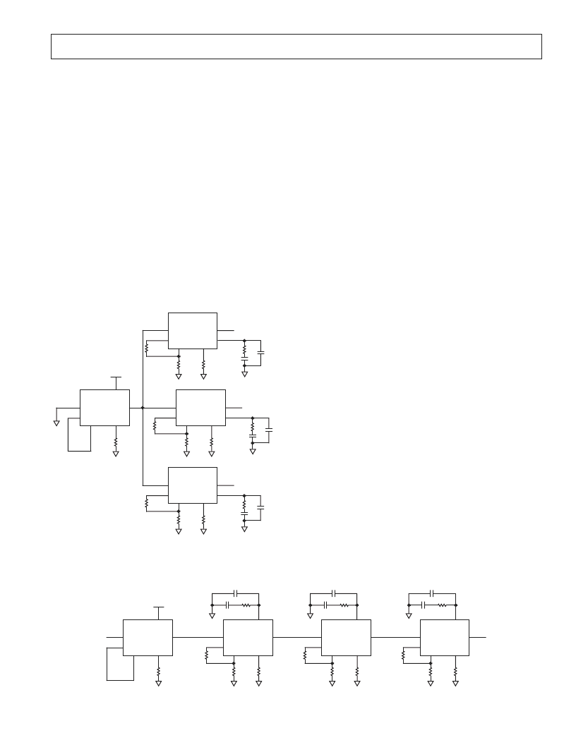
Figure 7. Multiple ADN8830 Devices Driven from
a Master Clock
Soft Start on Power-Up
The ADN8830 can be programmed to ramp up for a specified
time after the power supply is applied or after shutdown is
de-asserted. This feature, known as soft start, is useful for
gradually increasing the duty cycle of the PWM amplifier. The
soft start time is set with a single capacitor connected from Pin 27
to ground according to Equation 14.
τ
SS
SS
C
=
×
150
(14)
where
C
SS
is the value of the capacitor in microfarads, and
SS
is
the soft start time in milliseconds. To set a soft start time of 15 ms,
C
SS
should equal 0.1
μ
F. A minimum soft start time of 10 ms is
recommended to ensure proper initialization of the ADN8830
on power-up.
Shutdown Mode
The ADN8830 has a shutdown mode that deactivates the output
stage and puts the device into a low current standby state. The
current draw for the ADN8830 in shutdown is less than 100
μ
A.
The shutdown input, Pin 3, is active low. To shut down the
device, Pin 3 should be driven to logic low. Once a logic high is
applied, the ADN8830 will reactivate after the delay set by the
soft start circuitry. Refer to the Soft Start on Power-Up section
for more details on this feature.
Pin 3 should not be left floating as there are no internal pull-up
or pull-down resistors. If the shutdown function is not required,
Pin 3 should be tied to V
DD
to ensure the device is always active.
Compensation Loop
The ADN8830 TEC controller has a built-in amplifier dedicated
for loop compensation. The exact compensation network is set
by the user and can vary from a simple integrator to PI, PID, or
any other type of network. The type of compensation and com-
ponent values should be determined by the user since it will
depend on the thermal response of the object and the TEC. One
method for determining these values empirically is to input a step
function to TEMPSET, thus changing the target temperature,
and adjusting the compensation network to minimize the set-
tling time of the object
’
s temperature.
A typical compensation network used for temperature control
of a laser module is a PID loop, which consists of a very low
frequency pole and two separate zeros at higher frequencies.
Figure 9 shows a simple network for implementing PID com-
pensation. An additional pole is added at a higher frequency
than the zeros to reduce the noise sensitivity of the control loop.
The bode plot of the magnitude is shown in Figure 10.
29
6
ADN8830
MASTER
25
NC
26
R
FREQ
ADN8830
SLAVE
25
29
26
1.5M
28
50k
7
150k
28
25
29
26
1.5M
28
50k
7
150k
25
29
26
1.5M
28
50k
7
150k
NC
V
DD
24
24
24
24
1k
0.1 F
1nF
1k
0.1 F
1nF
1k
0.1 F
1nF
ADN8830
SLAVE
ADN8830
SLAVE
Figure 8. Multiple ADN8830 Devices Using a Daisy Chain
相關PDF資料 |
PDF描述 |
|---|---|
| FDR840 | P-Channel 2.5V Specified PowerTrench MOSFET |
| FDR840P | P-Channel 2.5V Specified PowerTrench MOSFET |
| FDR842P | P-Channel 1.8V Specified PowerTrench MOSFET |
| FDR844P | P-Channel 1.8V Specified PowerTrench MOSFET |
| FDR8508P | Dual P-Channel, Logic Level, PowerTrench⑩ MOSFET |
相關代理商/技術參數 |
參數描述 |
|---|---|
| FDW2520C | 制造商:Fairchild Semiconductor Corporation 功能描述:TSSOP-8 COMPLEMENTARY NCH 20V 300AGA |
| FDW2520C | 制造商:Fairchild Semiconductor Corporation 功能描述:MOSFET |
| FDW2520C_08 | 制造商:FAIRCHILD 制造商全稱:Fairchild Semiconductor 功能描述:Complementary PowerTrench MOSFET |
| FDW2520C_Q | 功能描述:MOSFET PowerTrench RoHS:否 制造商:STMicroelectronics 晶體管極性:N-Channel 汲極/源極擊穿電壓:650 V 閘/源擊穿電壓:25 V 漏極連續電流:130 A 電阻汲極/源極 RDS(導通):0.014 Ohms 配置:Single 最大工作溫度: 安裝風格:Through Hole 封裝 / 箱體:Max247 封裝:Tube |
| FDW2521C | 功能描述:MOSFET 20V/-20V N/P RoHS:否 制造商:STMicroelectronics 晶體管極性:N-Channel 汲極/源極擊穿電壓:650 V 閘/源擊穿電壓:25 V 漏極連續電流:130 A 電阻汲極/源極 RDS(導通):0.014 Ohms 配置:Single 最大工作溫度: 安裝風格:Through Hole 封裝 / 箱體:Max247 封裝:Tube |
發布緊急采購,3分鐘左右您將得到回復。