- 您現(xiàn)在的位置:買賣IC網(wǎng) > PDF目錄375780 > FDW2520C (Analog Devices, Inc.) Thermoelectric Cooler Controller PDF資料下載
參數(shù)資料
| 型號(hào): | FDW2520C |
| 廠商: | Analog Devices, Inc. |
| 英文描述: | Thermoelectric Cooler Controller |
| 中文描述: | 熱電冷卻器控制器 |
| 文件頁(yè)數(shù): | 21/24頁(yè) |
| 文件大小: | 416K |
| 代理商: | FDW2520C |
第1頁(yè)第2頁(yè)第3頁(yè)第4頁(yè)第5頁(yè)第6頁(yè)第7頁(yè)第8頁(yè)第9頁(yè)第10頁(yè)第11頁(yè)第12頁(yè)第13頁(yè)第14頁(yè)第15頁(yè)第16頁(yè)第17頁(yè)第18頁(yè)第19頁(yè)第20頁(yè)當(dāng)前第21頁(yè)第22頁(yè)第23頁(yè)第24頁(yè)
REV. C
ADN8830
–21–
Using an RTD for Temperature Sensing
The ADN8830 can be used with a resistive temperature device
(RTD) as the temperature feedback sensor. The resistance of an
RTD is linear with respect to temperature, offering an advan-
tage over thermistors that have an exponential relationship to
temperature. A constant current applied through an RTD will
yield a voltage proportional to temperature. However, this volt-
age could be on the order of only 0.5 mV/
°
C, thus requiring the
use of additional amplification to achieve a usable signal level.
The ADT70 from Analog Devices can be used to bias and amplify
the voltage across an RTD, which can then be fed directly to the
THERMIN pin on the ADN8830 to provide temperature
feedback for the TEC controller. The ADT70 uses a 0.9 mA
current source to drive the RTD and an instrumentation ampli-
fier with adjustable gain to boost the RTD voltage. Application
notes and typical schematics for this device can be found in the
ADT70 Data Sheet.
Most RTDs have a positive temperature coefficient, also called
tempco, as opposed to thermistors, which have a negative tempco.
For the OUT A output to drive the TEC
–
input as shown in
Figure 1, the signal from an RTD must be conditioned to create
a negative tempco. This can be easily done using an inverting
amplifier. Alternately, OUT A can be connected to drive TEC+
with OUT B driving TEC
–
with a positive tempco at THERMIN.
This is highlighted in the Output Driver Amplifiers section.
For the ADN8830, proper operation care should be taken
to ensure the voltage at THERMIN remains within 0.4 V
and 2.0 V. Using a 1 k
RTD with the ADT70 will yield a
THERMIN voltage of 0.9 V at 25
°
C. Using the application
circuit shown in Figure 22 will provide a nominal output
voltage of 1.0 V at 25
°
C and a total gain of 66.7 mV/
.
Using an RTD with a temperature coefficient of 0.375
/
°
C
will give a THERMIN voltage swing from 1.5 V at 5
°
C to
0.5 V at 45
°
C, well within the input range of the ADN8830.
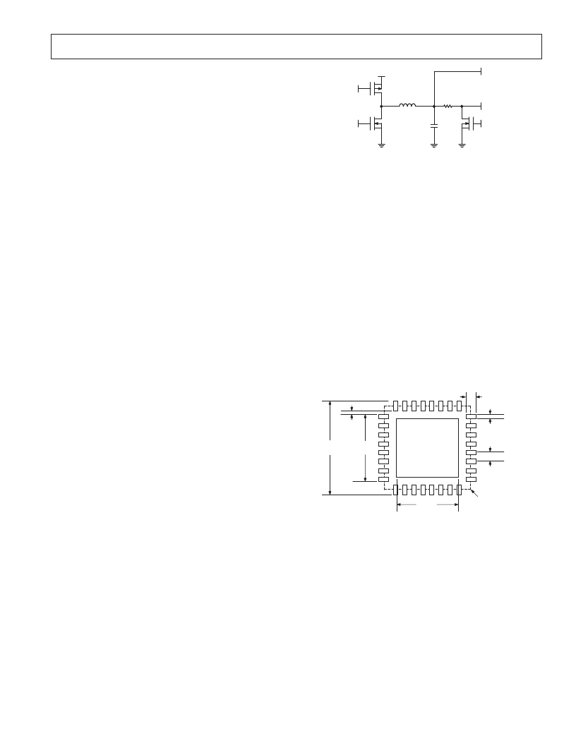
Using a Resistive Load as a Heating Element
The ADN8830 can be used in applications that do not neces-
sarily drive a TEC but require only a high current output into a
load resistance. Such applications generally only require heating
above ambient temperature and simply use the power dissipated
by the load element to accomplish this. Because the power
dissipated by such an element is proportional to the square of
the output voltage, the ADN8830 application circuit must be
modified. Figure 24 shows the preferred method for driving a
heating element load.
OUT B
C1
R
L
L1
PVDD
P1
Q1
N1
Q2
N2
Q3
OUT A
NO CONNECTION TO P2 REQUIRED
Figure 24. Using the ADN8830 to Drive a Heating Element
Current is delivered from the PWM amplifier through Q3 when
the voltage at THERMIN is lower than TEMPSET. If the object
temperature is greater than the target temperature, Q3 will turn
off and the current through the load goes to zero, allowing the
object to cool back toward the ambient temperature. As the
target temperature is approached, a steady output current should
be reached. Naturally, a proper compensation network must be
found to ensure stability and adequate temperature settling time.
The P2 output from the ADN8830 should be left unconnected.
Suggested Pad Layout for CP-32 Package
Figure 25 shows the dimensions for the PC board pad layout for
the ADN8830, which is a 5 5, 32-lead lead frame chipscale
package. This package has a metallic heat slug that should be
soldered to a copper pad on the PC board. Although the pack-
age slug is electrically connected to the substrate of the IC, the
copper pad should be left electrically floating. This prevents
potential noise injection into the substrate while maintaining
good thermal conduction to the PC board.
0.10
(0.0039)
3.78
(0.1488)
5.36
(0.2110)
3.68
(0.1449)
0.28
(0.0110)
0.50
(0.0197)
0.69
(0.0272)
CONTROLLING DIMENSIONS ARE IN MILLIMETERS; INCH DIMENSIONS
(IN PARENTHESES) ARE ROUNDED-OFF MILLIMETER EQUIVALENTS FOR
REFERENCE ONLY AND ARE NOT APPROPRIATE FOR USE IN DESIGN
THERMAL PAD SHOULD BE SOLDERED TO AN ELECTRICALLY FLOATING
PAD ON THE PC BOARD
PACKAGE
OUTLINE
Figure 25. Suggested PC Board Layout for CP-32
Pad Landing
相關(guān)PDF資料 |
PDF描述 |
|---|---|
| FDR840 | P-Channel 2.5V Specified PowerTrench MOSFET |
| FDR840P | P-Channel 2.5V Specified PowerTrench MOSFET |
| FDR842P | P-Channel 1.8V Specified PowerTrench MOSFET |
| FDR844P | P-Channel 1.8V Specified PowerTrench MOSFET |
| FDR8508P | Dual P-Channel, Logic Level, PowerTrench⑩ MOSFET |
相關(guān)代理商/技術(shù)參數(shù) |
參數(shù)描述 |
|---|---|
| FDW2520C | 制造商:Fairchild Semiconductor Corporation 功能描述:TSSOP-8 COMPLEMENTARY NCH 20V 300AGA |
| FDW2520C | 制造商:Fairchild Semiconductor Corporation 功能描述:MOSFET |
| FDW2520C_08 | 制造商:FAIRCHILD 制造商全稱:Fairchild Semiconductor 功能描述:Complementary PowerTrench MOSFET |
| FDW2520C_Q | 功能描述:MOSFET PowerTrench RoHS:否 制造商:STMicroelectronics 晶體管極性:N-Channel 汲極/源極擊穿電壓:650 V 閘/源擊穿電壓:25 V 漏極連續(xù)電流:130 A 電阻汲極/源極 RDS(導(dǎo)通):0.014 Ohms 配置:Single 最大工作溫度: 安裝風(fēng)格:Through Hole 封裝 / 箱體:Max247 封裝:Tube |
| FDW2521C | 功能描述:MOSFET 20V/-20V N/P RoHS:否 制造商:STMicroelectronics 晶體管極性:N-Channel 汲極/源極擊穿電壓:650 V 閘/源擊穿電壓:25 V 漏極連續(xù)電流:130 A 電阻汲極/源極 RDS(導(dǎo)通):0.014 Ohms 配置:Single 最大工作溫度: 安裝風(fēng)格:Through Hole 封裝 / 箱體:Max247 封裝:Tube |
發(fā)布緊急采購(gòu),3分鐘左右您將得到回復(fù)。