- 您現(xiàn)在的位置:買賣IC網(wǎng) > PDF目錄375780 > FDW2520C (Analog Devices, Inc.) Thermoelectric Cooler Controller PDF資料下載
參數(shù)資料
| 型號(hào): | FDW2520C |
| 廠商: | Analog Devices, Inc. |
| 英文描述: | Thermoelectric Cooler Controller |
| 中文描述: | 熱電冷卻器控制器 |
| 文件頁數(shù): | 12/24頁 |
| 文件大小: | 416K |
| 代理商: | FDW2520C |
REV. C
–12–
ADN8830
The unity-gain crossover frequency of the feedforward amplifier
is given as
f
R3 1
π
TEC GAIN
dB
0
1
2
80
=
×
×
(15)
To ensure stability, the unity-gain crossover frequency should be
lower than the thermal time constant of the TEC and thermistor.
However, this thermal time constant may not be specified and
can be difficult to characterize.
There are many texts written on loop stabilization, and it is beyond
the scope of this data sheet to discuss all methods and trade-offs
in optimizing compensation networks. A simple method that
can be used to empirically determine a PID compensation loop
as shown in Figure 9 involves the following procedure:
1. Connect thermistor and TEC to the ADN8830 application
circuit. Power does not need to be applied to the laser diode
for this procedure. Monitor output voltage across the TEC
with an oscilloscope.
2. Short C1 and open C2, leaving just R1 and R3 as a simple
proportional-only compensation loop.
3. While maintaining a constant TEMPSET voltage, increase
the ratio of R1/R3, thus increasing the gain until loop oscilla-
tion starts to occur. Decrease this ratio by a factor of 2 from
the point of oscillation. The R1/R3 ratio will likely be less
than unity for most laser modules.
4. Add C1 capacitor and decrease value until oscillation starts,
then increase by a factor of 2. A good initial starting value for
C1 is to create a unity-gain crossover of 0.1 Hz based on
Equation 15.
5. Short R2 and increase C2 until oscillation starts. At this point,
either C2 can be decreased or R2 can be added to regain
stability. Generally speaking, R2 will be greater than R3 and
C2 will be one or more orders of magnitude less than C1.
6. TEMPSET should be adjusted with a step change while
observing the output voltage settling time. A step change of
100 mV should suffice. From here, C2, R2, and even C1 can
be decreased to minimize settling time at the expense of
additional output voltage overshoot.
7. An additional feedback capacitor, CF, in parallel with R1
and C1, can be added to add another high frequency pole. In
many cases, this improves the stability of the system without
increasing the settling time as out-of-band noise is filtered
out of the control signal. A 330 pF to 1 nF capacitor should
suffice, if required.
The typical values shown in the typical application circuit in
Figure 1 have R1 = 100 k
, R2 = 1 M
, R3 = 205 k
, C1 = 10
μ
F
,
C2 = 1
μ
F, and an additional feedback capacitor of 330 pF. For
most pump laser modules, this results in a 10
°
C TEMPSET step
settling time to within 0.1
°
C in less than 5 seconds.
ADN8830
12
COMPOUT
TEMPCTL
COMPFB
13
R3
R2
R1
C1
14
C2
REFERENCE
VOLTAGE
CF
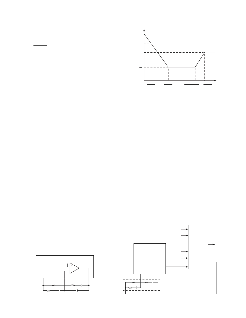
Figure 9. Implementing a PID Compensation Loop
FREQUENCY (Hz LOG SCALE)
R1
R3
M
R1
R2||R3
1
2 R1C1
1
2 C2(R2+R3)
1
2 R2C2
0dB
1
2 R3C1
Figure 10. Bode Plot for PID Compensation
Using the TEC Controller ADN8830 with a Wave Locker
Many optical applications require precision control of laser
wavelength. The wavelength of the laser diode can be adjusted
by changing its temperature, which is done through temperature
control of the TEC. Wavelength control can be done by feeding
a wave locker or etalon output back to the microprocessor and
using the microprocessor to calculate and reinstruct the TEC
controller with a new target temperature. However, this method
is computationally expensive and has time delays before the
adjustment is done. A faster responding and simpler method is
to feed the wave locker signal back to the TEC controller for
direct temperature control.
The ADN8830 is designed to be compatible with a wave locker
controller. Figure 11 shows the basic schematic. The TEMPCTL
output from ADN8830 is proportional to the object
’
s actual
temperature. This voltage is fed to the wave locker controller.
Also fed to the wave locker controller are the photodiode out-
puts from the wave locker, as well as the laser diode power and
a digital signal indicating a functional laser diode, both of which
come from the CW controller. The output of the wave locker
controller is then connected to the input of the compensation
network. This allows the wave locker controller to adjust the
TEC temperature based on the current temperature of the
object, the current wavelength of the laser diode, and the target
wavelength. Once the target wavelength is reached, the wave
locker controller sends a signal to the microcontroller indicating
that the laser signal is good.
ADN8830
COMPOUT
14
COMPFB
13
COMPENSATION
NETWORK
TEMPCTL
12
TEMP IN
LOCKER
PD1
LOCKER
PD2
LASER DIODE
POWER
LASER DIODE
GOOD
FROM
LOCKER
FROM CW
CONTROLLER
WAVE LOCKER
GOOD
TO
MICRO-
PROCESSOR
TEC
CONTROL
Figure 11. Using the ADN8830 with a Wave Locker
相關(guān)PDF資料 |
PDF描述 |
|---|---|
| FDR840 | P-Channel 2.5V Specified PowerTrench MOSFET |
| FDR840P | P-Channel 2.5V Specified PowerTrench MOSFET |
| FDR842P | P-Channel 1.8V Specified PowerTrench MOSFET |
| FDR844P | P-Channel 1.8V Specified PowerTrench MOSFET |
| FDR8508P | Dual P-Channel, Logic Level, PowerTrench⑩ MOSFET |
相關(guān)代理商/技術(shù)參數(shù) |
參數(shù)描述 |
|---|---|
| FDW2520C | 制造商:Fairchild Semiconductor Corporation 功能描述:TSSOP-8 COMPLEMENTARY NCH 20V 300AGA |
| FDW2520C | 制造商:Fairchild Semiconductor Corporation 功能描述:MOSFET |
| FDW2520C_08 | 制造商:FAIRCHILD 制造商全稱:Fairchild Semiconductor 功能描述:Complementary PowerTrench MOSFET |
| FDW2520C_Q | 功能描述:MOSFET PowerTrench RoHS:否 制造商:STMicroelectronics 晶體管極性:N-Channel 汲極/源極擊穿電壓:650 V 閘/源擊穿電壓:25 V 漏極連續(xù)電流:130 A 電阻汲極/源極 RDS(導(dǎo)通):0.014 Ohms 配置:Single 最大工作溫度: 安裝風(fēng)格:Through Hole 封裝 / 箱體:Max247 封裝:Tube |
| FDW2521C | 功能描述:MOSFET 20V/-20V N/P RoHS:否 制造商:STMicroelectronics 晶體管極性:N-Channel 汲極/源極擊穿電壓:650 V 閘/源擊穿電壓:25 V 漏極連續(xù)電流:130 A 電阻汲極/源極 RDS(導(dǎo)通):0.014 Ohms 配置:Single 最大工作溫度: 安裝風(fēng)格:Through Hole 封裝 / 箱體:Max247 封裝:Tube |
發(fā)布緊急采購,3分鐘左右您將得到回復(fù)。