- 您現在的位置:買賣IC網 > PDF目錄375864 > FMS7401LEN (FAIRCHILD SEMICONDUCTOR CORP) Digital Power Controller PDF資料下載
參數資料
| 型號: | FMS7401LEN |
| 廠商: | FAIRCHILD SEMICONDUCTOR CORP |
| 元件分類: | 微控制器/微處理器 |
| 英文描述: | Digital Power Controller |
| 中文描述: | 8-BIT, EEPROM, 2.04 MHz, MICROCONTROLLER, PDIP8 |
| 封裝: | PLASTIC, DIP-8 |
| 文件頁數: | 19/80頁 |
| 文件大小: | 1535K |
| 代理商: | FMS7401LEN |
第1頁第2頁第3頁第4頁第5頁第6頁第7頁第8頁第9頁第10頁第11頁第12頁第13頁第14頁第15頁第16頁第17頁第18頁當前第19頁第20頁第21頁第22頁第23頁第24頁第25頁第26頁第27頁第28頁第29頁第30頁第31頁第32頁第33頁第34頁第35頁第36頁第37頁第38頁第39頁第40頁第41頁第42頁第43頁第44頁第45頁第46頁第47頁第48頁第49頁第50頁第51頁第52頁第53頁第54頁第55頁第56頁第57頁第58頁第59頁第60頁第61頁第62頁第63頁第64頁第65頁第66頁第67頁第68頁第69頁第70頁第71頁第72頁第73頁第74頁第75頁第76頁第77頁第78頁第79頁第80頁
PRODUCT SPECIFICATION
FMS7401/7401L
REV. 1.0.2 6/23/04
19
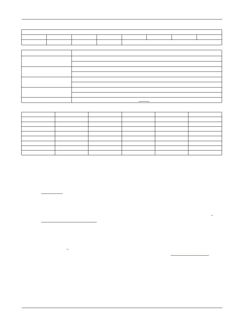
Table 5. ADCNTRL1 Register Bit Definitions
Table 6. Analog Input Channel Selection (ACHSEL[3:0]) Bit Definitions
ACHSEL[3]
ACHSEL[2]
0
0
0
0
0
0
0
0
1
0
1
0
1
0
1
1
4.1.2 ADCNTRL2 Register
The ADCNTRL2 is an 8-bit memory map register used to configure the analog circuits. Six of the eight register bits are used to
configure circuits directly related to the ADC circuit while the others are not related.
Bit 7 (REFBY2) of the ADCNTRL2 register is the reference clock (F
RCLK1
) divide-by-2 enable bit. The REFBY2 bit config-
ures the reference clock of the PLL and Programmable Comparator circuit to be sourced either by F
RCLK1
or F
RCLK1
/2 clock.
Refer to the
Clock Circuit
section of the datasheet for additional details.
Bit 6 (COMPSEL) of the ADCNTRL2 register is the Programmable Comparator’s non-inverting input selection bit. If
COMPSEL=0, the non-inverting input of the Programmable Comparator is the G4/AIN0 device pin. If COMPSEL=1, the
non-inverting input of the Programmable Comparator is the G2/AIN2 device pin. Before enabling the Programmable
Comparator circuit, the selected analog input port pin must be configured as a tri-state input bypassing the I/O circuitry.
9
Refer to the
Programmable Comparator Circuit
section of the datasheet for addition details.
Bit 5 of the ADCNTRL2 register is the Uncommitted Amplifier Enable (ENAMP) bit. If ENAMP=0, the Uncommitted Ampli-
fier circuit is disabled and its pin connections (G6/-A
IN
and G7/A
OUT
) may be used as normal I/O ports. The G7/AIN4 pin may
still be used as a standard ADC conversion input through the analog ACH5 channel. If ENAMP=1, the Uncommitted Amplifier
circuit is enabled and its pin connections must be configured as tri-state inputs where G6/-A
IN
is the inverting input and G7/
A
OUT
is the amplifier output.
9
If the ADC circuit is performing a conversion on the analog ACH5 input when driven by the
Uncommitted Amplifier, software must avoid clearing the ENAMP bit. Refer to the following
Uncommitted Amplifier
section
for additional details.
Bit 4 (ENDAS) of the ADCNTRL2 register enables the ADC conversion’s gated auto-sampling operating mode. If ENDAS=1,
the ADC circuit configures the F
ADCLK
clock for synchronization with the PWM Timer 1’s ADSTROBE output signal. The
ADC circuit will then accept triggers by the active (on) edge transition of the ADSTROBE signal. All other ADC configuration
ADCNTRL1 Register (addr. 0x9F)
Bit 4
REFSEL
Bit 7
APND
Bit 6
AINTEN
Bit 5
ASTART
Bit 3
Bit 2
Bit 1
Bit 0
ACHSEL[3:0]
Bit
APND
Description
(0) ADC’s pending flag is cleared.
(1) ADC’s pending flag is triggered.
(0) Disables ADC hardware interrupts.
(1) Enables ADC hardware interrupts.
(0) ADC conversion is not in progress.
(1) Start an ADC conversion / ADC conversion in progress.
(0) ADC Reference (V
AREF
) = Internal V
REF
(1) ADC Reference (V
AREF
) = Vcc
Analog Input Channel Selection Bits. Refer to
Table 6
for details.
AINTEN
ASTART
REFSEL
ACHSEL[3:0]
ACHSEL[1]
0
0
1
1
0
0
1
0
ACHSEL[0]
0
1
0
1
0
1
0
0
Analog Channel
ACH1
ACH2
ACH3
ACH4
ACH5
AGND
+V
REF
Vcc/3
I/O Equiv.
G4/AIN0
G3/AIN1
G2/AIN2
G1/AIN3
G7/AIN4/A
OUT
-
-
-
相關PDF資料 |
PDF描述 |
|---|---|
| FMS7401LEN14 | Digital Power Controller |
| FMS7401LVN | Digital Power Controller |
| FMS7401LVN14 | Digital Power Controller |
| FMS7G10US60S | SWTCH ROLLER SPDT 20A SCRW TERM |
| FMS7G10US60 | SWTCH ROLLER SPDT 20A SOLD TERM |
相關代理商/技術參數 |
參數描述 |
|---|---|
| FMS7401LEN14 | 功能描述:處理器 - 專門應用 Int Controller for Ballast RoHS:否 制造商:Freescale Semiconductor 類型:Multimedia Applications 核心:ARM Cortex A9 處理器系列:i.MX6 數據總線寬度:32 bit 最大時鐘頻率:1 GHz 指令/數據緩存: 數據 RAM 大小:128 KB 數據 ROM 大小: 工作電源電壓: 最大工作溫度:+ 95 C 安裝風格:SMD/SMT 封裝 / 箱體:MAPBGA-432 |
| FMS7401LEN14_Q | 功能描述:處理器 - 專門應用 Int Controller for Ballast RoHS:否 制造商:Freescale Semiconductor 類型:Multimedia Applications 核心:ARM Cortex A9 處理器系列:i.MX6 數據總線寬度:32 bit 最大時鐘頻率:1 GHz 指令/數據緩存: 數據 RAM 大小:128 KB 數據 ROM 大小: 工作電源電壓: 最大工作溫度:+ 95 C 安裝風格:SMD/SMT 封裝 / 箱體:MAPBGA-432 |
| FMS7401LVN | 功能描述:處理器 - 專門應用 Int Controller for Ballast RoHS:否 制造商:Freescale Semiconductor 類型:Multimedia Applications 核心:ARM Cortex A9 處理器系列:i.MX6 數據總線寬度:32 bit 最大時鐘頻率:1 GHz 指令/數據緩存: 數據 RAM 大小:128 KB 數據 ROM 大小: 工作電源電壓: 最大工作溫度:+ 95 C 安裝風格:SMD/SMT 封裝 / 箱體:MAPBGA-432 |
| FMS7401LVN14 | 功能描述:8位微控制器 -MCU Int Controller for Ballast RoHS:否 制造商:Silicon Labs 核心:8051 處理器系列:C8051F39x 數據總線寬度:8 bit 最大時鐘頻率:50 MHz 程序存儲器大小:16 KB 數據 RAM 大小:1 KB 片上 ADC:Yes 工作電源電壓:1.8 V to 3.6 V 工作溫度范圍:- 40 C to + 105 C 封裝 / 箱體:QFN-20 安裝風格:SMD/SMT |
| FMS7401LVN14_Q | 功能描述:8位微控制器 -MCU Int Controller for Ballast RoHS:否 制造商:Silicon Labs 核心:8051 處理器系列:C8051F39x 數據總線寬度:8 bit 最大時鐘頻率:50 MHz 程序存儲器大小:16 KB 數據 RAM 大小:1 KB 片上 ADC:Yes 工作電源電壓:1.8 V to 3.6 V 工作溫度范圍:- 40 C to + 105 C 封裝 / 箱體:QFN-20 安裝風格:SMD/SMT |
發布緊急采購,3分鐘左右您將得到回復。