- 您現在的位置:買賣IC網 > PDF目錄375914 > FS6054 (Electronic Theatre Controls, Inc.) LOW-SKEW CLOCK FANOUT BUFFER ICs PDF資料下載
參數資料
| 型號: | FS6054 |
| 廠商: | Electronic Theatre Controls, Inc. |
| 英文描述: | LOW-SKEW CLOCK FANOUT BUFFER ICs |
| 中文描述: | 低偏移時鐘扇出緩沖器集成電路 |
| 文件頁數: | 18/19頁 |
| 文件大小: | 386K |
| 代理商: | FS6054 |
XT
April 1999
4.5.99
18
)6)6)6)6
/RZ6NHZ&ORFN)DQRXW%XIIHU,&V
,62
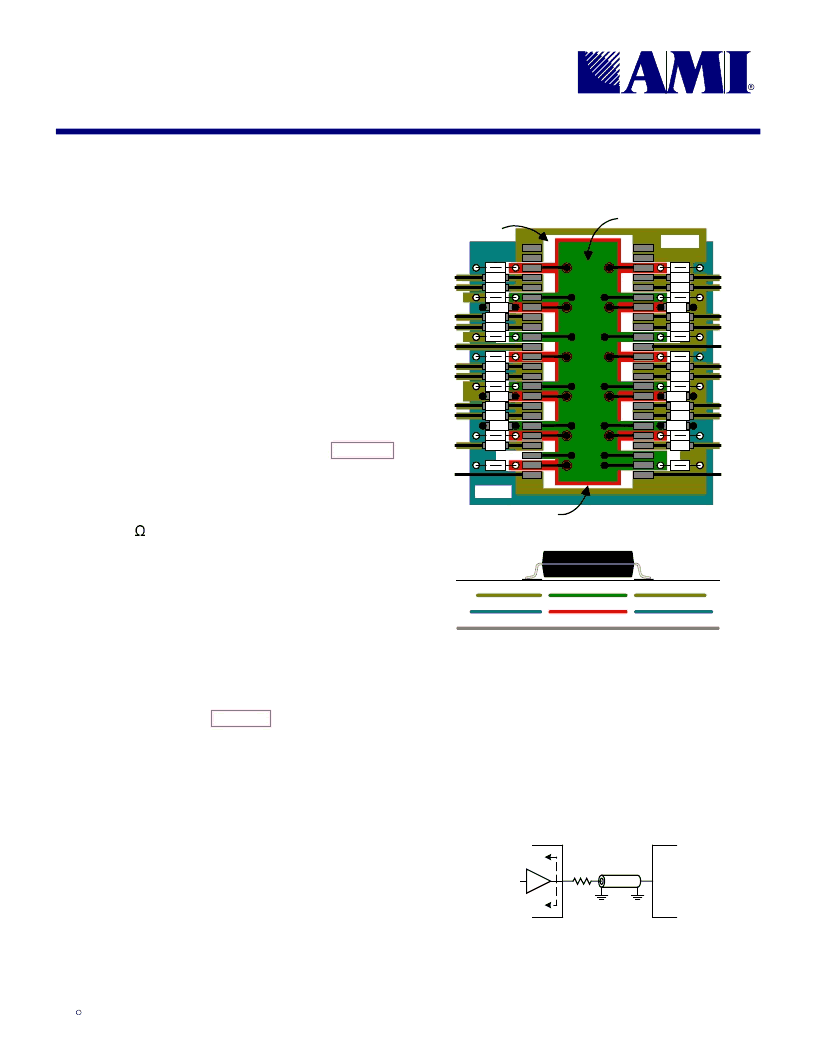
8.0 Application Information
8.1
The primary concern when designing the board layout for
this device is the reduction of electromagnetic interfer-
ence (EMI) generated by the 18 copies of the 100MHz
SDRAM clock. It is assumed the reader is familiar with
basic transmission line theory.
Reduction of EMI
8.1.1
To obtain the best performance, noise should be mini-
mized on the power and ground supplies to the IC. Ob-
serve good high-speed board design practices, such as:
Use multi-layer circuit boards with dedicated low im-
pedance power and ground planes for the device
(denoted as CLK VDD and CLK GND in Figure 18).
The device power and ground planes should be
completely isolated from the motherboard power and
ground planes by a void in the power planes.
Several low-pass filters using low impedance ferrite
EHDGV
DW0+]DUHUHFRPPHQGHGWRGHFR
ple the device power and ground planes from the
motherboard power and ground planes (MB VDD and
MB GND). The beads should span the gap between
the power and ground planes. Seven beads for
power and seven beads for ground are suggested
(14 total) so that the clock rise times (1V/ns) can be
maintained.
Place 1000pF bypass capacitors as close as possible
to the power pins of the IC. Use RF-quality low-
inductance multi-layer ceramic chip capacitors. Six
capacitors is optimal, one on each power/ground
grouping as shown in Figure 18.
Load similar clock outputs equally, and keep output
loading as light as possible to help reduce clock skew
and power dissipation.
Use equal-length clock traces that are as short as
possible. Rounded trace corners help reduce reflec-
tions and ringing in the clock signal.
The clock traces must never cross the void area be-
tween power/ground planes. Each trace must have a
complete plane (either VDD or GND) under the com-
plete length of the trace.
Layout Guidelines
u-
Figure 18: Board Layout
1
2
4
5
8
9
11
13
14
17
18
21
48
45
41
40
36
28
25
47
MB GND
MB VDD
31
32
44
35
38
24
CLK GND
CLK VDD
VOID
R
S
R
S
1000pF
1000pF
1000pF
1000pF
1000pF
1000pF
CLK GND
CLK VDD
MB GND
MB GND
MB VDD
MB VDD
Signal Layer
Component
Layer
R
S
R
S
R
S
R
S
R
S
R
S
R
S
R
S
R
S
R
S
R
S
R
S
R
S
R
S
R
S
R
S
8.1.2
A signal reflection will occur at any point on a PC-board
trace where impedance mismatches exist. Reflections
cause several undesirable effects in high-speed applica-
tions, such as an increase in clock jitter and a rise in
electromagnetic emissions from the board. Using a prop-
erly designed series termination on each high-speed line
can alleviate these problems by eliminating signal reflec-
tions.
Output Driver Termination
Figure 19: Series Termination
R
S
z
L
z
O
DRIVER
RECEIVE
LINE
相關PDF資料 |
PDF描述 |
|---|---|
| FS6131-01 | Programmable Line Lock Clock Generator IC |
| FS6282 | DUAL PLL CLOCK GENERATOR IC |
| FS6282-03 | DUAL PLL CLOCK GENERATOR IC |
| FS6M07652RTC | Time-Delay Relay; Contacts:SPST-NO; Time Range:0.2 sec. to 20 sec.; Timing Function:Delay-On-Make; Voltage Rating:120V |
| FS6M07652RTCTU | Fairchild Power Switch(FPS) |
相關代理商/技術參數 |
參數描述 |
|---|---|
| FS605NA | 制造商:NETGEAR 功能描述:FS605NA FAST ENET SWITCH 制造商:NETGEAR 功能描述:NETGEAR FS605 - Switch - 5 x 10/100 - desktop |
| FS6070-01 | 制造商:未知廠家 制造商全稱:未知廠家 功能描述:Buffer/Driver |
| FS608NA | 制造商:TECH DATA 功能描述:NETGEAR FS608 - Switch - 8 x 10/100 - desktop |
| FS608UK | 制造商:NETGEAR 功能描述:SWITCH 10/100 8PORT UK ADADATER 制造商:NETGEAR 功能描述:SWITCH, 10/100, 8PORT, UK ADADATER |
| FS-60A | 制造商:Distributed By MCM 功能描述:Foot Pedal Switch |
發布緊急采購,3分鐘左右您將得到回復。